
Manufacturing Process

Fifteen controlled stages carry a bare panel from incoming laminate to a tested, packed board. Every stage has a named owner, a documented acceptance check and a record that travels with the order — so what you approve at the front end is what you receive at the back end. Comprehensive CAM data audit and expert-led DFM reviews, ensuring your complex designs are fully optimized for production readiness. 100% verification of incoming laminates with full batch traceability, guaranteeing a certified technical foundation. Precision panel cutting of copper-clad laminates into exact blank sizes, maximizing material utilization. Advanced LDI laser imaging for ultra-fine inner layer circuits, followed by mandatory AOI inspection. Precise vacuum pressing with 100% inner-layer AOI before bonding, guaranteeing flawless interlayer registration. Automated CNC and laser drilling supporting 0.1mm micro-vias for high-frequency designs. Automated plating lines ensure uniform copper thickness and reliable conductivity in high-aspect-ratio holes. Outer layer circuit patterning followed by high-precision AOI inspection of traces and pads. High-grade solder mask application exposing only the pads, ensuring oxidation resistance and solderability. Premium ENIG / ENEPIG surface finishing for maximum oxidation resistance and peak solderability. Precision CNC router profiling separates boards from the panel with smooth, clean edges. Total netlist verification via flying probe or fixture testing, guaranteeing zero open or short defects. Final visual inspection with magnifying lamp and light table, verifying every board before release. Final quality audit with stamping release approval, confirming compliance before shipment. ESD-safe vacuum packing in anti-static bags and sturdy cartons for secure global delivery. Twelve stages take a bare board from solder-paste printing to a tested, packed assembly. Each one is inspected before the next begins — paste volume, placement, joints and function — so a defect is caught at the station that created it, not at final test. Technical review of Gerber and BOM files to optimize design and prevent production errors. 100% inspection and verification of incoming materials with full batch traceability. Fully automated stencil printing for precise solder volume control on every pad. High-speed 3D Solder Paste Inspection to verify height and volume before placement. High-precision placement of 01005 chips and 0.3mm pitch BGAs at ±25μm accuracy. 10-zone soldering in an oxygen-free environment to ensure bright, void-free joints. Dual-stage automated optical inspection to detect any visual or soldering defects. Non-destructive 3D X-Ray inspection to verify BGA and hidden solder joint integrity. Targeted through-hole soldering to protect sensitive components from thermal stress. Automated application of protective layers for high-reliability in extreme environments. 100% closed-loop validation of electrical connectivity and logic functionality. Full system integration and ESD-safe packaging for immediate global delivery. Files are reviewed against the process that will build them — minimum trace and spacing, annular ring, aspect ratio and copper balance — before release, not after first article. Prototype and volume orders run through the same 15-step flow, with panelization, tooling and stack-up settled before the first panel is cut. Built to IPC-6012 Class 3, with AOI, X-Ray and electrical test records kept against every order. Files are reviewed against the process that will build them, before the order is released.Making a PCB — Step by Step

Engineering DFM Review
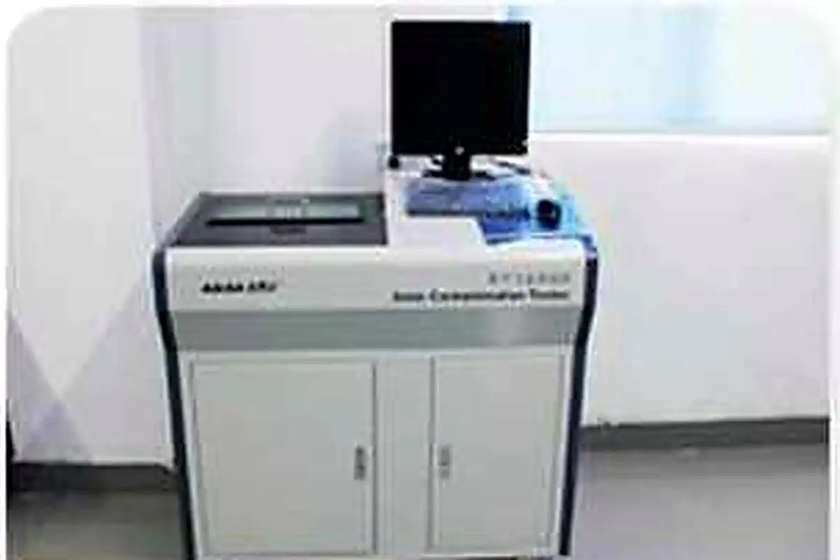
Material Integrity & IQC
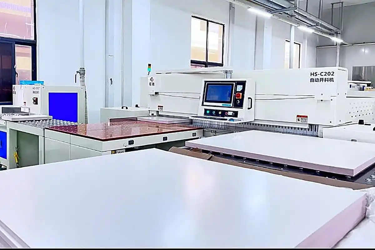
Board Cutting
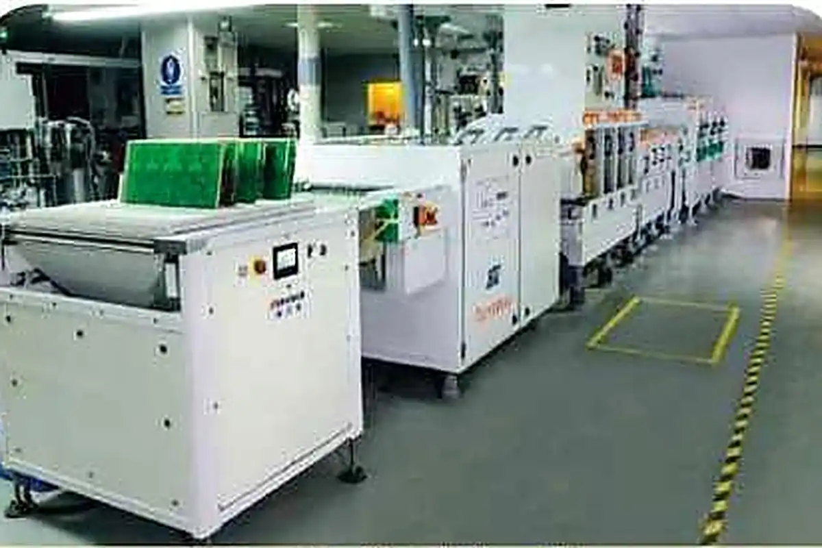
Inner Layer Imaging (LDI) & AOI
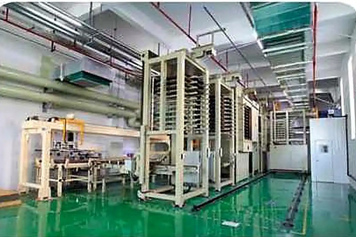
Structural Lamination & AOI
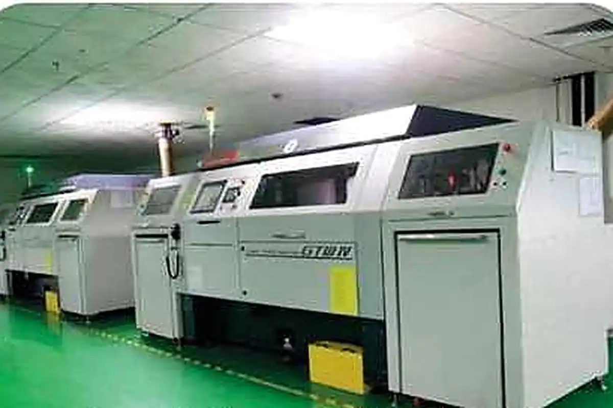
High-Precision Drilling
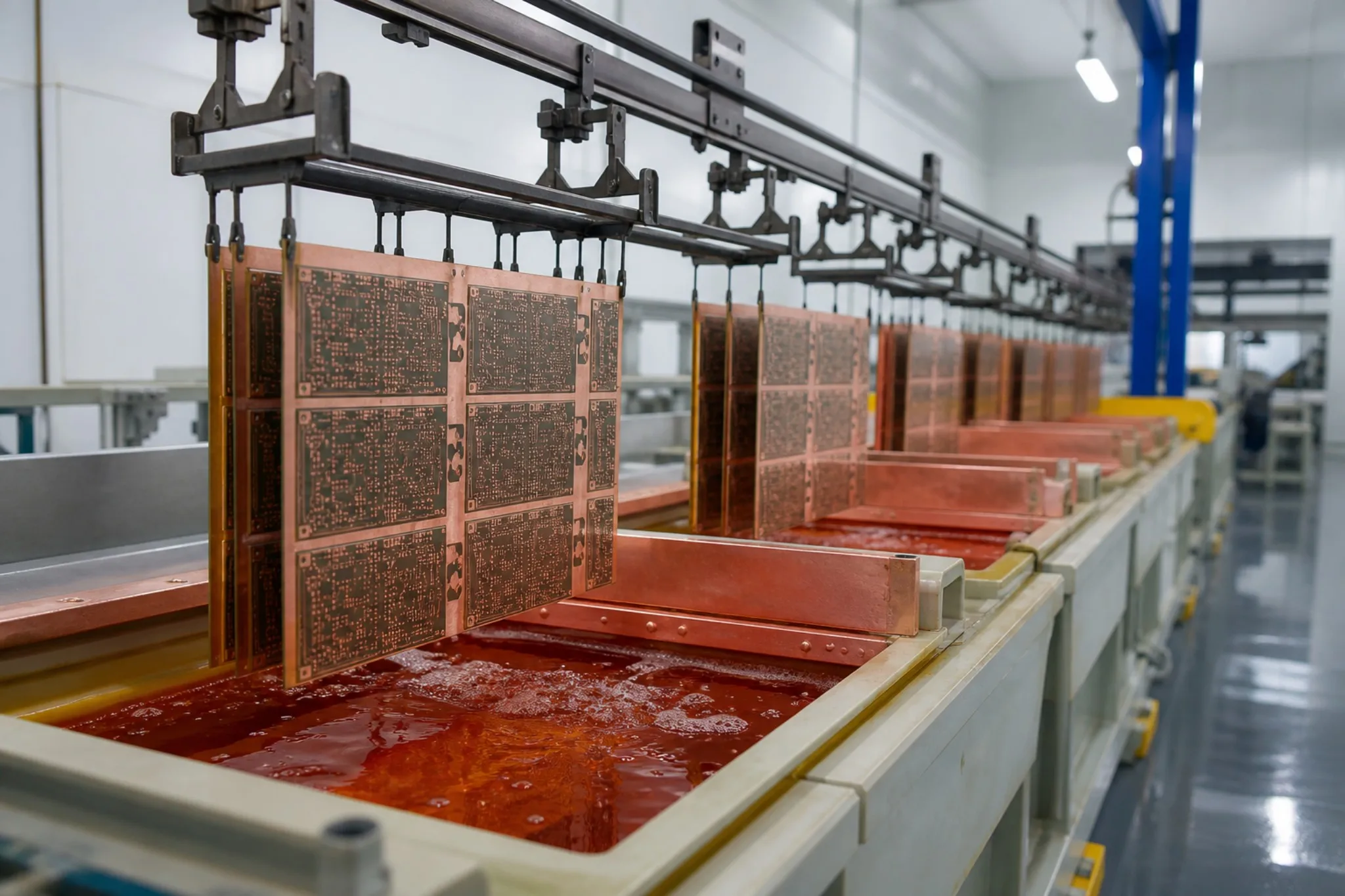
Copper Plating & PTH
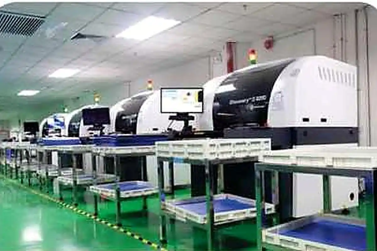
Outer Layer Imaging & AOI
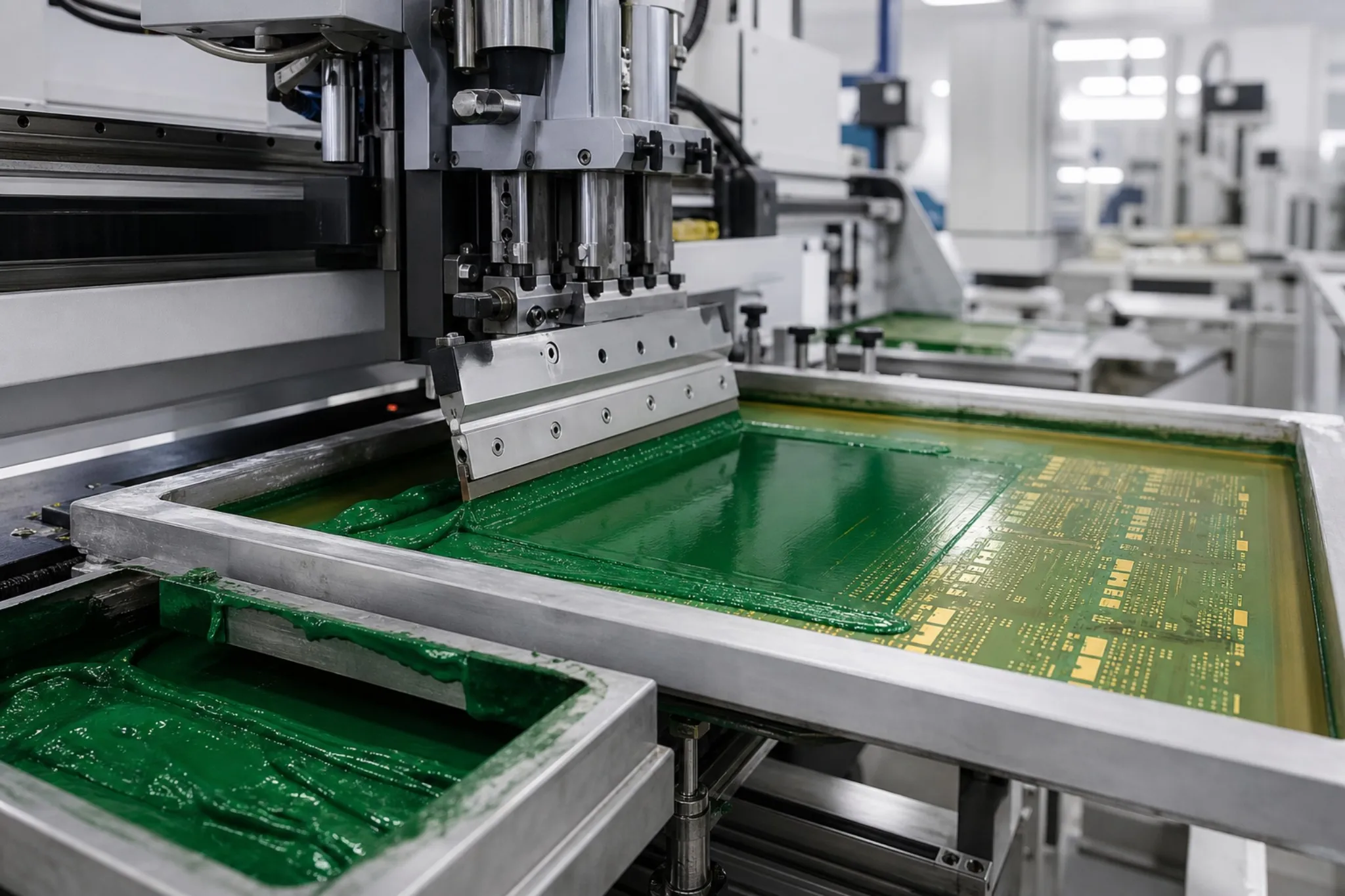
Solder Mask
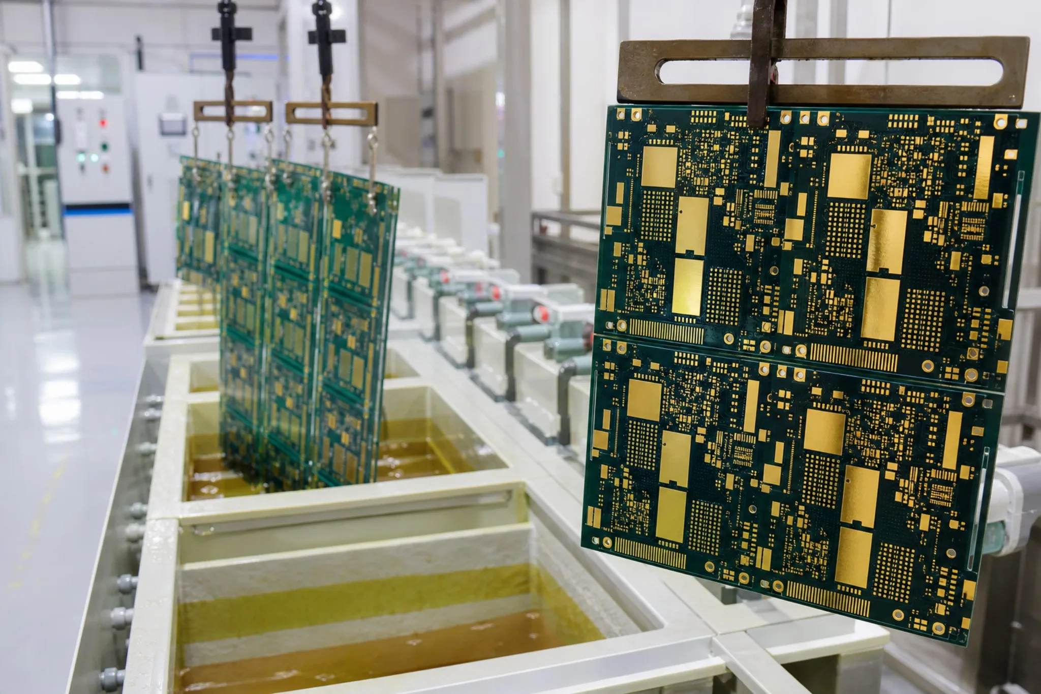
Surface Finish
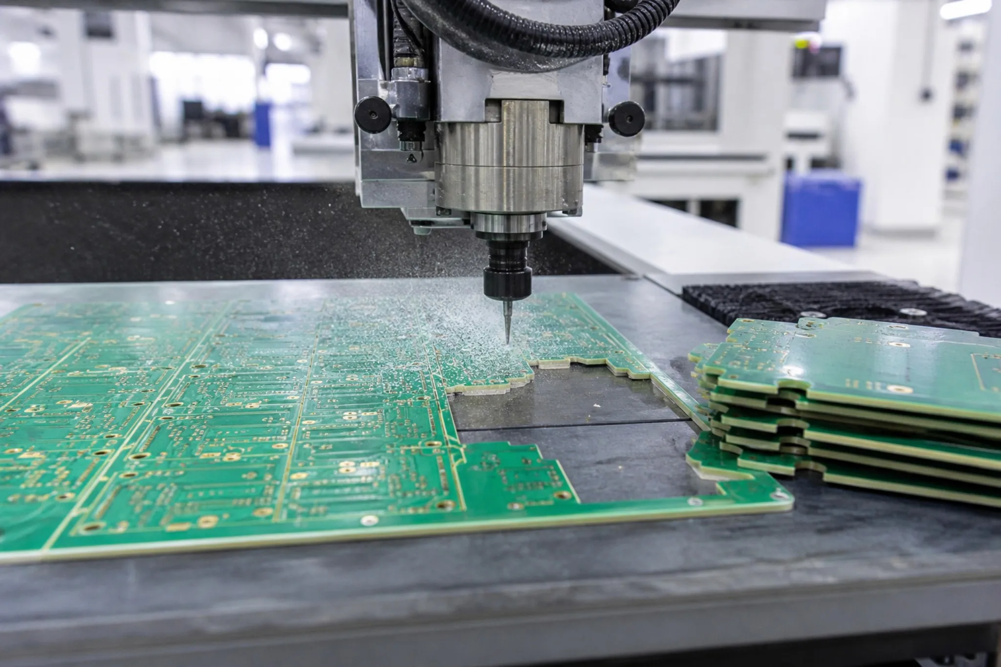
Routing & Profiling
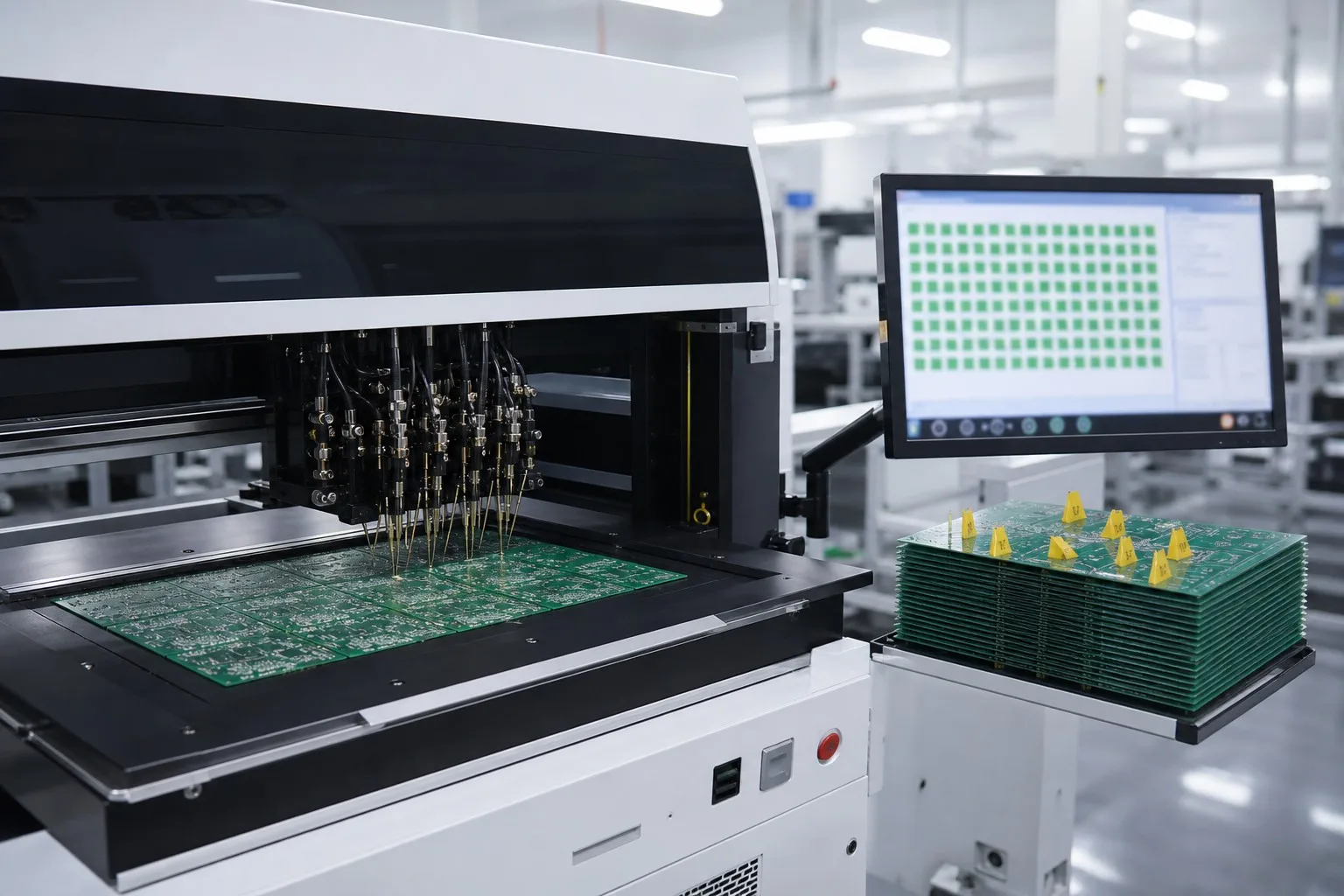
100% Electrical Test
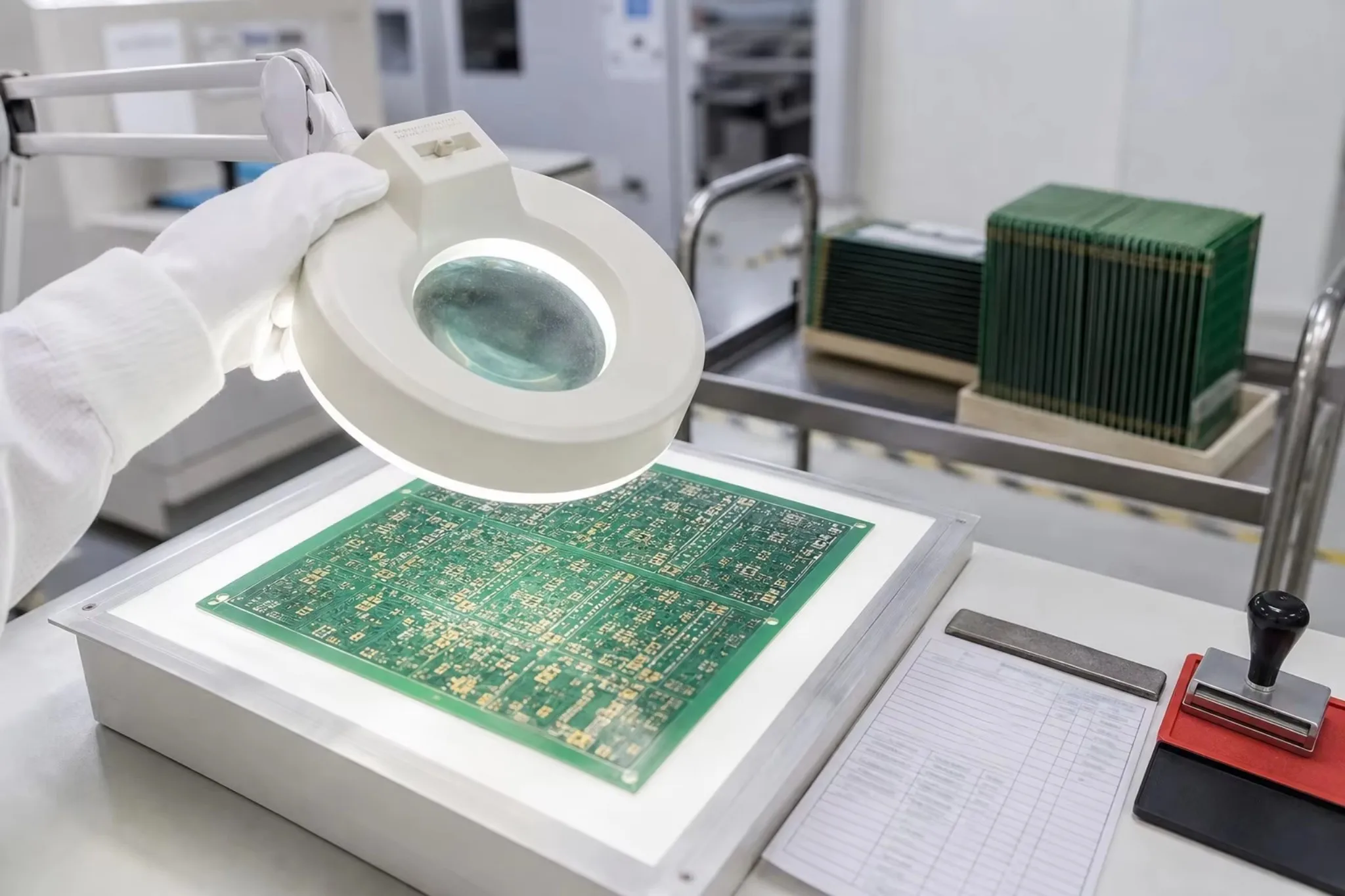
FQC (Final Quality Control)
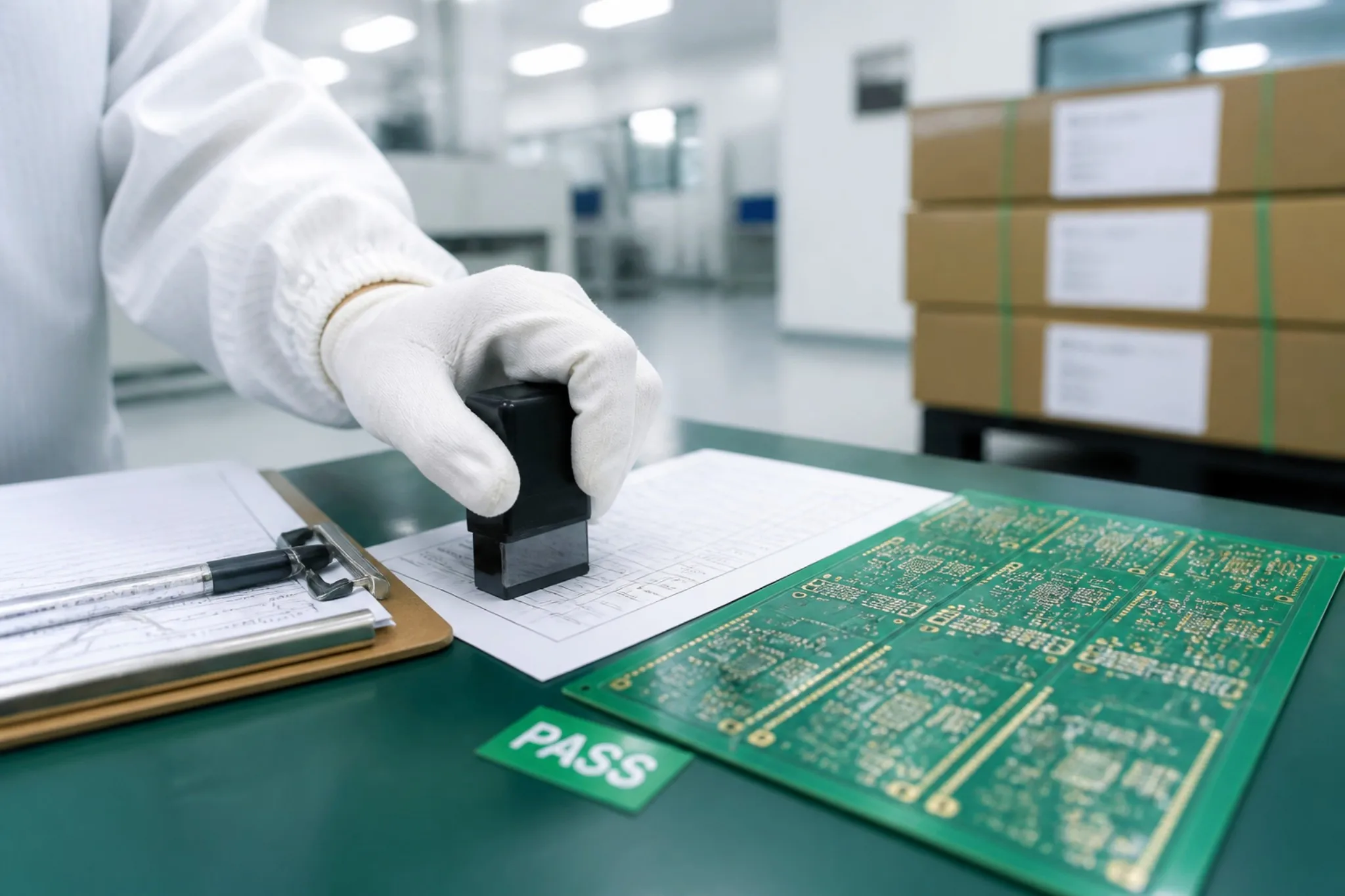
FQA (Final Quality Assurance)
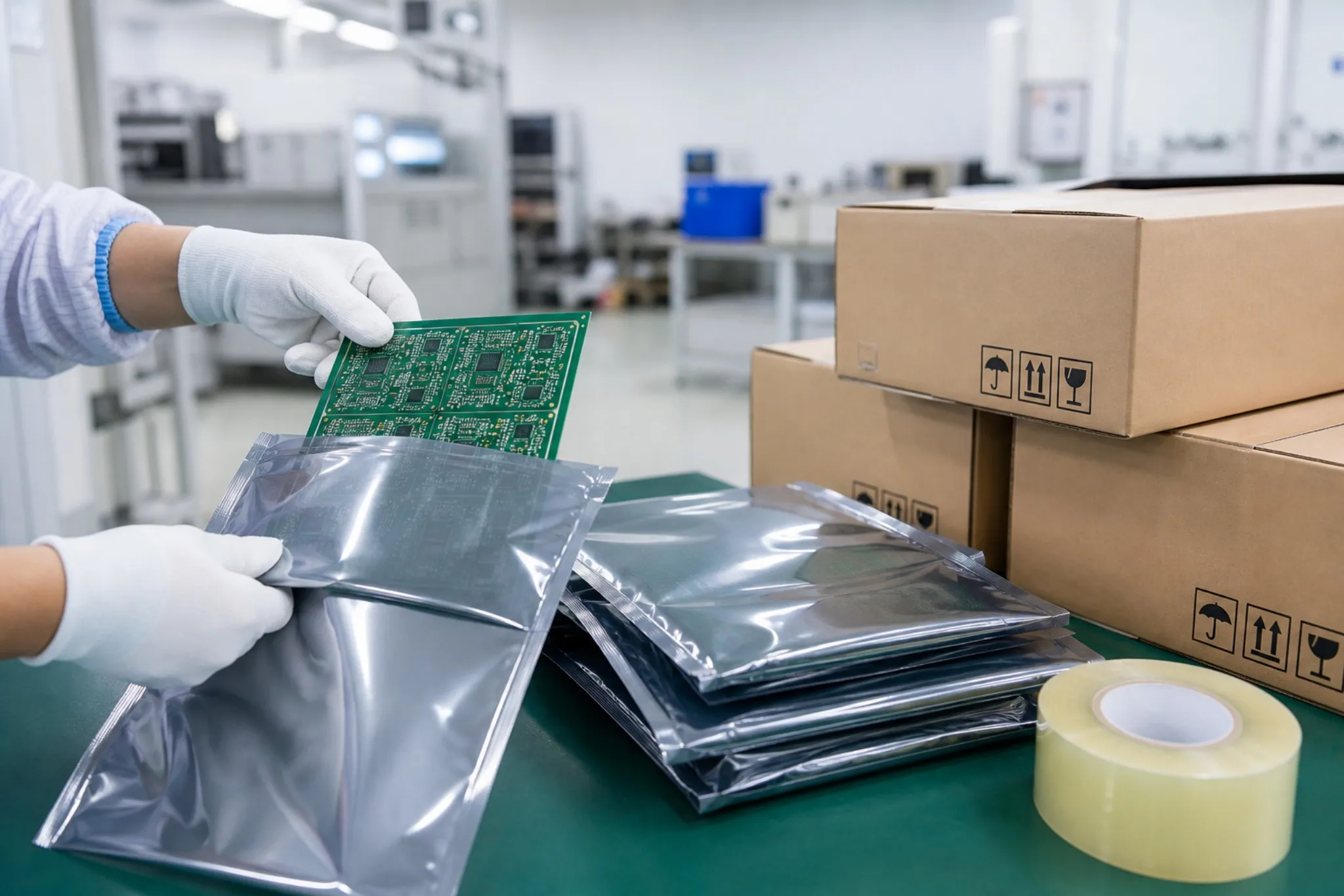
Secure Packing
PCBA Assembly: From DFM Audit to Box-Build

Engineering Audit & DFM

Component IQC & Management

Precision Solder Paste Printing

3D Solder Paste Inspection (SPI)

High-Speed SMT Placement

Nitrogen (N2) Reflow Soldering

Dual-Stage 3D AOI Inspection

3D X-Ray & CT Integrity Audit

THT & Selective Soldering

Conformal Coating & Potting

ICT & Functional Test (FCT)

System Box-Build & Packing

Engineering Expertise

Scalable Solutions

Verified Reliability
