


What is the principle of PCB multi-layer board selection?
PCB laminated structure design has a direct impact on product cost and product EMC. The increase of the board layer facilitates the wiring, but also increases the cost. When designing, it is necessary to consider various requirements to achieve the best balance.
After completing the pre-layout of components, it is generally necessary to focus on the analysis of the PCB wiring bottlenecks. Combine with other EDA tools to analyze the wiring density of the circuit board; then synthesize the number and types of signal lines with special wiring requirements, such as differential lines, sensitive signal lines, etc., to determine the number of signal layers; then according to the type of power supply, isolation and anti-interference The requirements to determine the number of internal electrical layers.
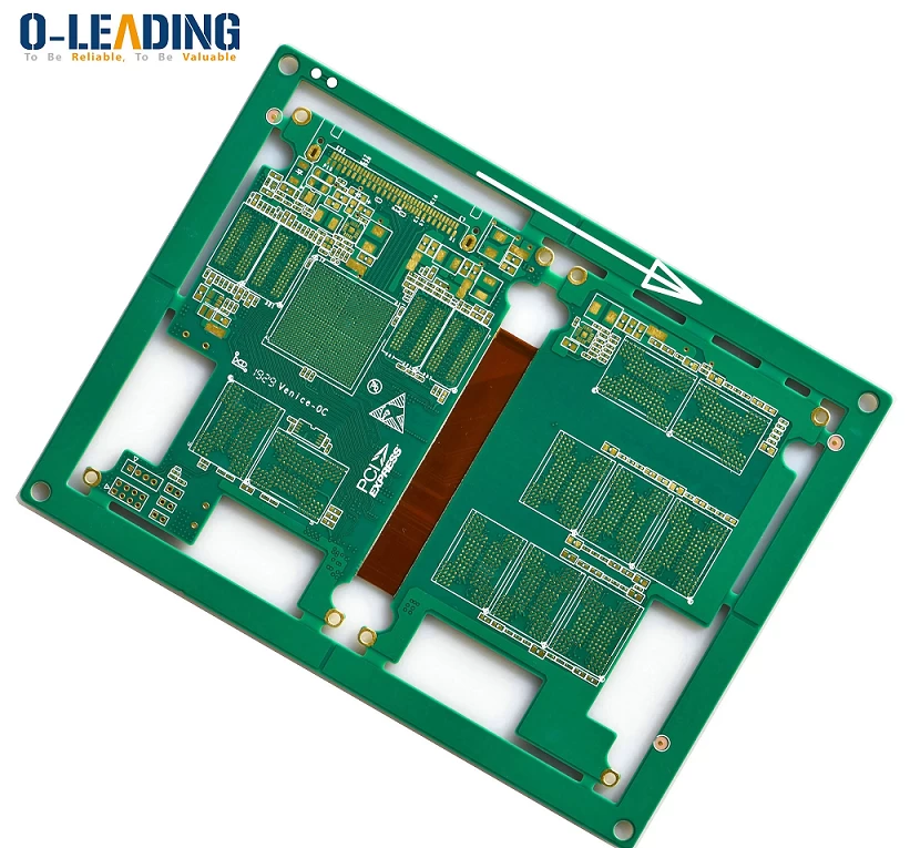
Factory Price multilayer rigid flexible HDI PCB Circuit Board
Consideration of cascading selection factors
The more layers of the circuit board, the more types of permutations and combinations of special signal layers, ground layers and power layers.
(1) The signal layer should be adjacent to an inner electric layer (internal power/ground layer), and the large copper film of the inner electric layer is used to provide shielding for the signal layer.
(2) The internal power supply layer and the ground layer should be tightly coupled, that is, the thickness of the medium between the internal power supply layer and the ground layer should be a smaller value.
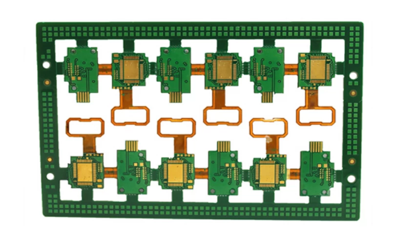
customized flex rigid pcb multilayer electronic pcb manufacturer
(3) The high-speed signal transmission layer in the circuit should be a signal intermediate layer and sandwiched between two inner electrical layers. In this way, the copper film of the two inner electric layers can provide electromagnetic shielding for high-speed signal transmission, and at the same time, it can effectively limit the radiation of high-speed signals between the two inner electric layers without causing external interference.
(4) Avoid two signal layers directly adjacent to each other. It is easy to introduce crosstalk between adjacent signal layers, resulting in circuit function failure. Adding a ground plane between the two signal layers can effectively avoid crosstalk.
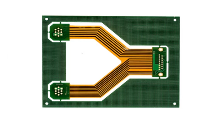
High quality China multilayer rigid flex PCB manufacturer
(5) Multiple grounded internal electrical layers can effectively reduce ground impedance. For example, the A signal layer and the B signal layer use separate ground planes, which can effectively reduce common mode interference.
(6) Taking into account the symmetry of the layer structure.