


Selective soldering and through-hole reflow soldering technology
Selective soldering
In selective soldering, only some specific areas are in contact with the solder wave. Since the PCB itself is a poor heat conduction medium, it will not heat and melt the solder joints of adjacent components and the PCB area during soldering. Flux must be pre-coated before soldering. Flux is only applied to the parts to be soldered on the lower part of the PCB, but selective soldering is not suitable for soldering SMD components.
Through hole reflow soldering
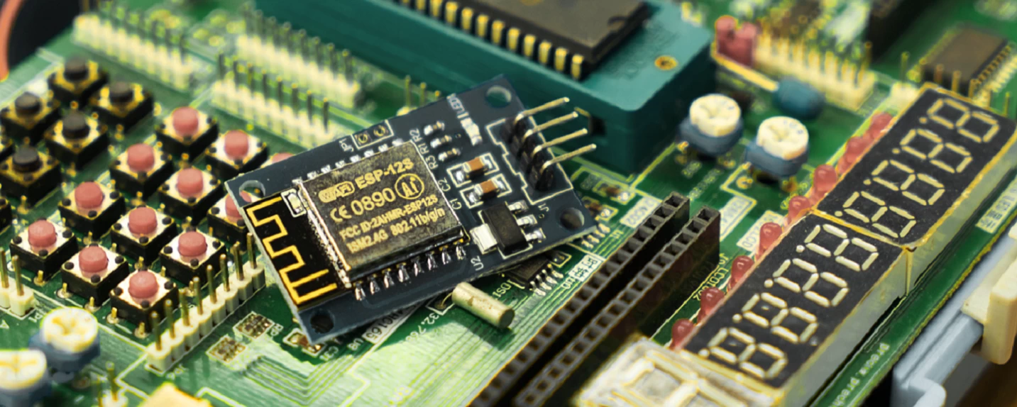
Through-hole reflow soldering process is to use reflow soldering technology to assemble through-hole components and special-shaped components. As products pay more and more attention to miniaturization, increased functionality and increased component density, many single-sided and double-sided panels are mainly surface-mounted components. However, due to factors such as inherent strength, reliability, and applicability, in some cases through-hole devices are still superior to SMC, especially connectors at the edge of the PCB.
double side through hole flexible circuit board folding high reliable quality fpcb type
The disadvantage of using through-hole devices on circuit boards with surface-mounted components is that the cost of a single solder joint is very high. For this type of assembly, the key is to be able to provide through-hole and surface-mounted components in a single integrated process. Provide synchronous reflow soldering.
Compared with the general surface mount process, the amount of solder paste used in the through-hole reflow process is more than that of the general SMT, which is about 30 times. Currently, the through-hole reflow process mainly adopts two solder paste coating technologies, including solder paste printing and automatic solder paste dispensing.
1. Solder paste printing
Screen printing is the preferred method of depositing solder paste on the PCB. The thickness of the stencil is a key factor, which will affect the amount of solder paste that is missed onto the PCB. A stepped mesh board can be used, where the thicker areas are designed for through-hole devices. This stencil design can meet the requirements of different solder paste volumes.
2. Automatically point solder paste
Auto-dot solder paste successfully deposits the correct volume of solder paste for through-holes and irregular components. It provides the flexibility and ability to deposit large amounts of solder paste that may not be possible with screen printing. When applying solder paste to the exposed plated through hole (PTH), it is recommended to use a nozzle with a slightly larger diameter than the PTH. In this way, when the solder paste is applied, the solder paste is forced to close to the hole wall of the PTH, and the material is slightly extruded from the bottom of the PTH, and then the component is inserted in the opposite direction of the solder paste. If you use a nozzle smaller than the PTH diameter, the solder paste will be discharged from the hole and cause serious solder paste loss.
Green Solder Mask ENIG PCB Board
Through-hole reflow soldering can replace wave soldering in many aspects to realize the soldering of plug-in components, especially the soldering of plug-in solder joints with high-density SMD components (or fine-pitch SMD) distributed on the soldering surface. Improve the welding quality, which is enough to make up for the lack of expensive equipment. The emergence of through-hole reflow soldering is of great help to enriching soldering methods, improving circuit board assembly density, improving soldering quality, and reducing process flow.