


How to deal with PCB board cooling
I. Analysis of temperature rise factors of printed circuit boards
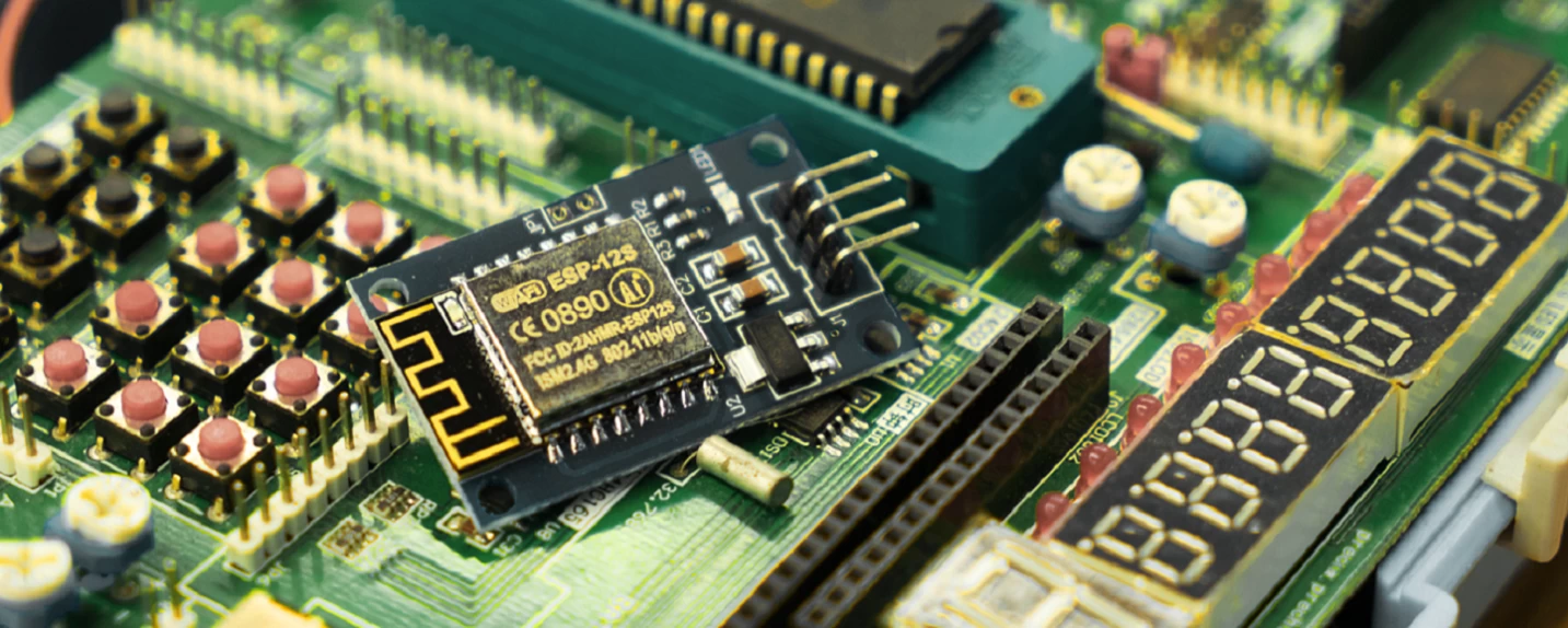
The direct cause of the temperature rise of the printed board is due to the existence of circuit power consumption devices. The electronic devices have different degrees of power consumption, and the heat generation intensity varies with the power consumption.
Engine Power Module manufacturer china
Two phenomena of temperature rise in printed boards:
(1) local temperature rise or large area temperature rise;
(2) Short-term temperature rise or long-term temperature rise.
When analyzing PCB thermal power consumption, it is generally analyzed from the following aspects.
Electrical power consumption
(1) Analysis of power consumption per unit area;
(2) Analyze the distribution of power consumption on the PCB board.
2. Printed board structure
(1) the size of the printed board;
(2) The material of the printed board.
3. How to install the printed board
(1) Installation method (such as vertical installation, horizontal installation);
(2) Sealing condition and distance from the casing.
4. Thermal radiation
(1) the emissivity of the surface of the printed board;
(2) the temperature difference between the printed board and the adjacent surface and their absolute temperature;
5 heat conduction
(1) installing a radiator;
(2) Conduction of other mounting structural members.
6. Heat convection
(1) Natural convection;
(2) Forced cooling convection.
The analysis of the above factors from the PCB is an effective way to solve the temperature rise of the printed board. These factors are often related and dependent in a product and system. Most of the factors should be analyzed according to the actual situation, only for a specific In actual conditions, parameters such as temperature rise and power consumption can be calculated or estimated correctly.
Second, the circuit board cooling method
1. High heat generating device with heat sink and heat conducting plate
When there are a few devices in the PCB that generate a large amount of heat (less than 3), a heat sink or a heat pipe can be added to the heat generating device. When the temperature cannot be lowered, a heat sink with a fan can be used to enhance heat dissipation. effect. When the amount of heat-generating devices is large (more than 3), a large heat-dissipating cover (plate) can be used, which is a dedicated heat sink customized according to the position and height of the heat-generating device on the PCB or a large flat-plate heat sink. The upper and lower parts of the different components are placed. The heat shield is integrally fastened to the component surface, and is in contact with each component to dissipate heat. However, due to the poor consistency of components during soldering, the heat dissipation effect is not good. A soft thermal phase change thermal pad is usually added to the component surface to improve heat dissipation.
2. Cooling through the PCB board itself
Currently widely used PCB sheets are copper-clad/epoxy glass cloth substrates or phenolic resin glass cloth substrates, and a small amount of paper-based copper-clad sheets are used. Although these substrates have excellent electrical properties and processing properties, they have poor heat dissipation. As a heat dissipation path for high-heat-generating components, it is hardly expected to conduct heat from the resin of the PCB itself, but to dissipate heat from the surface of the component to the surrounding air. However, as electronic products have entered the era of miniaturization, high-density mounting, and high-heat assembly, it is not enough to dissipate heat from the surface of a component with a very small surface area. At the same time, due to the large number of surface mount components such as QFP and BGA, the heat generated by the components is transferred to the PCB in a large amount. Therefore, the best way to solve the heat dissipation is to improve the heat dissipation capability of the PCB itself in direct contact with the heat generating components. Conducted out or emitted.
3. Use a reasonable wiring design to achieve heat dissipation
Since the resin in the sheet has poor thermal conductivity, and the copper foil line and the hole are good conductors of heat, increasing the copper foil residual ratio and increasing the heat conduction hole are the main means of heat dissipation.
To evaluate the heat dissipation capability of a PCB, it is necessary to calculate the equivalent thermal conductivity (nine eq) of a composite material composed of various materials having different thermal conductivity coefficients.
4. For devices that use free convection air cooling, it is best to arrange the integrated circuits (or other devices) in a vertically long manner or in a horizontally long manner.
5. Devices on the same printed board should be placed as far as possible according to their heat generation and heat dissipation. Devices with low heat or poor heat resistance (such as small signal transistors, small scale integrated circuits, electrolytic capacitors, etc.) should be placed. The uppermost flow (at the inlet) of the cooling airflow, the device that generates a large amount of heat or heat (such as a power transistor, a large-scale integrated circuit, etc.) is placed at the most downstream of the cooling airflow.
6. In the horizontal direction, the high-power devices are placed as close as possible to the edge of the printed board to shorten the heat transfer path; in the vertical direction, the high-power devices are placed as close as possible to the top of the printed board to reduce the temperature of other devices while these devices are operating. Impact.
7. Temperature sensitive devices should be placed in the lowest temperature area (such as the bottom of the device). Do not place it directly above the heating device. Multiple devices are preferably staggered on a horizontal plane.
8. The heat dissipation of the printed circuit board in the device mainly depends on the air flow, so the air flow path should be studied during the design, and the device or printed circuit board should be properly configured. When the air flows, it tends to flow in a place with low resistance. Therefore, when configuring the device on the printed circuit board, avoid leaving a large air space in a certain area. The same problem should be noted in the configuration of multiple printed circuit boards in the whole machine.
Consigned PCB Assembly factory
9. Avoid the concentration of hot spots on the PCB, distribute the power evenly on the PCB as much as possible, and keep the temperature performance of the PCB surface uniform and consistent. It is often difficult to achieve a strict uniform distribution during the design process, but it is necessary to avoid areas where the power density is too high, so as to avoid the hot spots affecting the normal operation of the entire circuit. If necessary, it is necessary to perform thermal performance analysis of printed circuits. For example, the thermal performance index analysis software modules added in some professional PCB design software can help designers optimize circuit design.
10. Place the device with the highest power consumption and maximum heat generation near the best location for heat dissipation. Do not place a device with a higher heat on the corners and peripheral edges of the printed board unless a heat sink is placed near it. When designing the power resistor, choose a larger device as much as possible, and have enough space for heat dissipation when adjusting the layout of the printed board.
11. High heat dissipation devices should minimize the thermal resistance between them when they are connected to the substrate. In order to better meet the thermal characteristics requirements, some thermal conductive materials (such as a layer of thermal silica gel) can be used on the bottom surface of the chip, and a certain contact area is maintained for the device to dissipate heat.
12. Device to substrate connection:
(1) Minimize the length of the device leads;
(2) When selecting a high-power device, the thermal conductivity of the lead material should be considered, and if possible, try to select the maximum cross-section of the lead;
(3) Select a device with a large number of pins.
Package selection for 13 devices:
(1) When considering thermal design, pay attention to the package description of the device and its thermal conductivity;
(2) Consideration should be given to providing a good thermal conduction path between the substrate and the device package;
(3) Air partitions should be avoided on the heat conduction path, and if this is the case, a heat conductive material can be used for filling.
O-Leading Supply Chain CO., LTD
TEL: + 86-752-8457668
Fax: + 86-4008892163-239121
+ 86-2028819702-239121