
Blog

PCB Surface Finish Selection: ENIG, ENEPIG, HASL, OSP, Immersion Silver and Tin Compared
PCB Surface Finish Selection: ENIG, ENEPIG, HASL, OSP, Immersion Silver and Tin Compared
Six finishes, four IPC specifications, and one decision that follows your board through assembly, storage and the field.
The surface finish is the last thing specified on a fabrication drawing and the first thing that decides whether assembly runs cleanly. It is a few tenths of a micron of metal or organic film on top of the copper — and it is the only part of the board whose job changes completely depending on how you measure it, how long you store it, and what you do to it next.
Most finish decisions are made by pattern-matching. Someone on the team used ENIG on the last project, so ENIG goes on this one. That works until a board fails for a reason nobody connects back to the finish: solder joints that looked perfect at AOI and cracked in thermal cycling, pads that wet poorly after eight months in a warehouse, gold fingers that go intermittent after a few hundred insertions.
This article is a selection guide, not a sales sheet. It walks through what each finish actually is at the deposit level, what the IPC specifications require, where each one fails, and how to defend the choice in a design review.
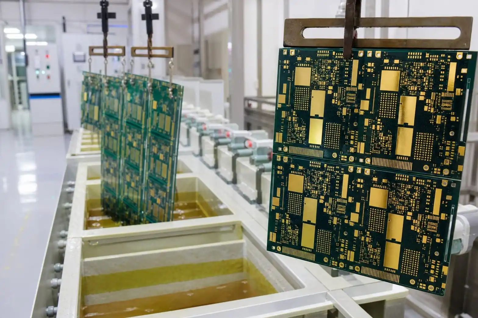
01 The Finish Is a System, Not a Coating
Three jobs, three different failure modes.
Every finish on a printed circuit board is asked to do three things at once, and the three jobs pull in different directions:
- Protect the copper while the board waits. Bare copper oxidizes. The window between fabrication and assembly can be two weeks or two years, and the finish is the only thing standing between the pad and the atmosphere.
- Wet properly on the first reflow. During reflow the finish must dissolve or displace cleanly so that molten solder reaches a metallurgically clean surface and forms a reliable intermetallic bond.
- Survive whatever comes after. Test probing, handling, conformal coating, connector mating, thermal cycling, humidity, and eventually the customer.
Because those jobs conflict, no single finish wins on all three. A thick, wear-resistant deposit is a poor reflow surface. A finish optimized for a one-time reflow is too soft for repeated mechanical contact. A sub-micron organic film that gives the flattest pads is also the one that consumes itself during assembly.
There is a fourth consideration that engineers often miss because it is not on the drawing: the finish determines which measurements are possible. Some finishes can be verified non-destructively on the shop floor with an X-ray fluorescence gauge; others cannot be measured on a finished board at all. If your acceptance criteria depend on a number, the finish choice decides whether that number can be checked.
What the specifications actually cover
The IPC plating subcommittee has published a separate final-finish specification for each of the finishes that reached industry consensus. Knowing which finishes have a specification — and which do not — is the fastest way to tell whether a supplier can be held to a number.
| Finish | IPC specification | First issued | What it fixes |
|---|---|---|---|
| ENIG — electroless nickel / immersion gold | IPC-4552 (Rev A 2017, Rev B 2021) | 2002 | Nickel and gold thickness, plus nickel corrosion evaluation from Rev A onward |
| Immersion silver | IPC-4553 (Rev A 2009) | 2005 | Single thickness window with both a minimum and a maximum |
| Immersion tin | IPC-4554 (amended 2011) | 2007 | Minimum thickness, solderability testing and flux conditions |
| ENEPIG — electroless nickel / electroless palladium / immersion gold | IPC-4556 (amended 2015) | 2013 | Nickel, palladium and gold thickness; upper gold limit added in 2015 |
| OSP — organic solderability preservative | None | — | No consensus was reached; see below |
| HASL — hot air solder leveling | None as a deposit specification | — | Thickness is set by the process, not by a target deposit |
One finish on this list has no specification at all. Work on an OSP specification — IPC-4555 — ran from 2008 for more than a year without reaching consensus, because the organic chemistries in commercial use differ too much in mechanism and recommended thickness. Section 06 covers what that means in practice.
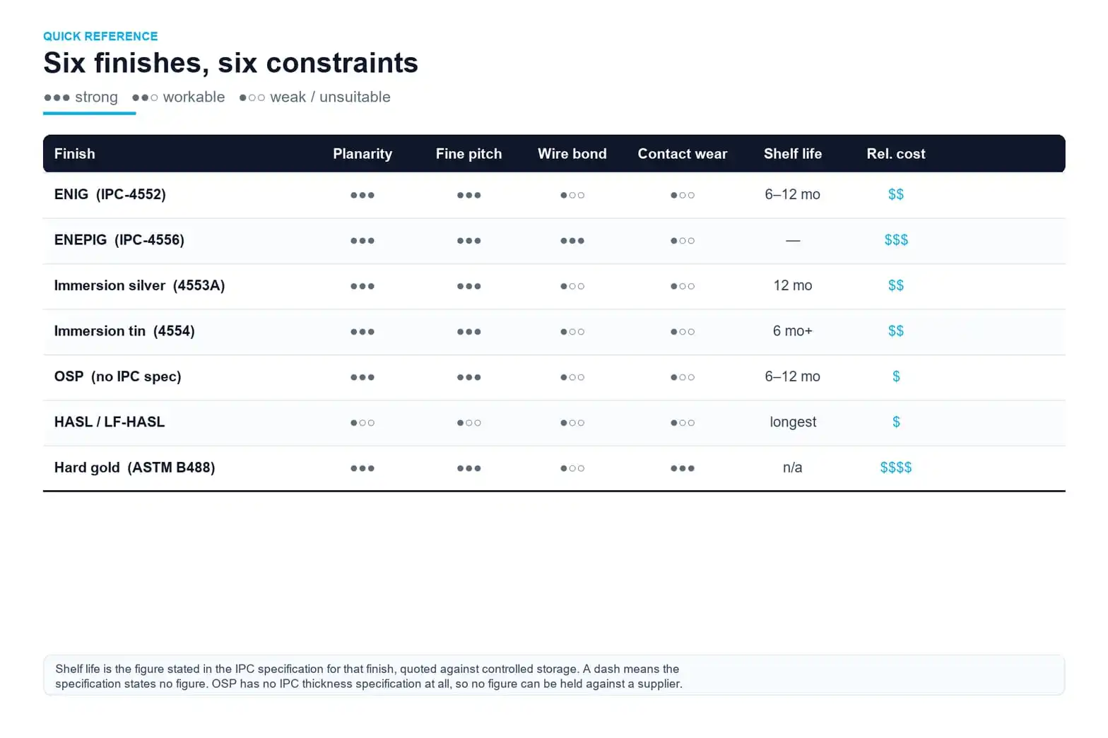
02 The Six Finishes at a Glance
What each one is, before we argue about which is better.
The table below is the quick orientation. Everything after it is the detail that actually decides the outcome.
| Finish | What it is | Specified thickness | Planarity | Typical role |
|---|---|---|---|---|
| HASL / lead-free HASL | Pads dipped in molten solder, then leveled by a hot air knife | Set by the process; varies with solder volume left after the air knife | Lowest — domed pads | Cost-driven boards with generous pitch |
| ENIG | Electroless nickel barrier capped with a very thin immersion gold layer | Ni 3–6 µm; Au 0.04–0.1 µm per IPC-4552A | High — flat pads | The general-purpose default for fine pitch and long shelf life |
| ENEPIG | ENIG with an electroless palladium layer inserted between nickel and gold | Ni 3–6 µm; Pd 0.05–0.30 µm; Au 0.03–0.07 µm per IPC-4556 | High | Boards that will be gold wire bonded as well as soldered |
| OSP | A sub-micron organic film that bonds to clean copper and protects it | No IPC specification; commonly run around 0.2–0.5 µm | Highest — film conforms to the copper | High-volume assembly with a short fabrication-to-assembly window |
| Immersion silver | Silver deposited directly onto copper by chemical displacement | 0.12–0.4 µm per IPC-4553A, typically 0.2–0.3 µm | High | Fine pitch with good solderability and moderate cost |
| Immersion tin | Tin deposited onto copper by chemical displacement | 1.0 µm minimum per IPC-4554, typically 1.15–1.3 µm | High | Press-fit and solderable surfaces where silver is undesirable |
03 ENIG: The Default, and Its One Real Failure Mode
Two layers, two jobs, and a defect that hides under a perfect surface.
ENIG is what most engineers reach for when they need flat pads, a long shelf life and a finish that works for both fine-pitch assembly and test. It is also the finish with the best-documented failure mode in the industry, and understanding that failure is the price of using it well.
What the two layers do
ENIG is a two-layer system and the layers do not share a job:
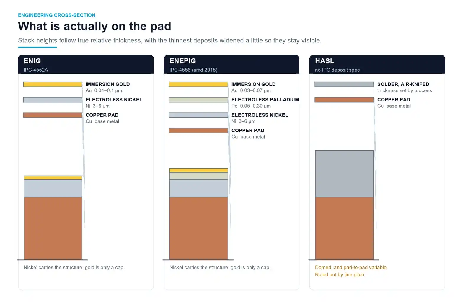
- The electroless nickel layer is the structural one. It sits between the copper and the solder and acts as a diffusion barrier, preventing copper from migrating into the joint during reflow. IPC-4552 specifies it at 3–6 µm for Classes 1, 2 and 3.
- The immersion gold is a protective cap, not a structural layer. Because it is deposited by chemical displacement — gold ions displacing nickel atoms, with the nickel itself supplying the electrons — deposition is self-limiting. The gold protects the nickel from oxidation during storage and provides the wettable surface. During reflow it dissolves rapidly into the molten solder, leaving the nickel to form the bond.
The numbers have moved over the life of the specification, and the movement is instructive. The original IPC-4552 set the gold minimum at 0.05 µm at four sigma below the mean, with a typical range of 0.075–0.125 µm and no upper limit. A 2012 amendment lowered the floor to 0.04 µm under restrictions. Then IPC-4552A, issued in 2017, did something the earlier revisions had not: it set an upper limit. Gold was specified at 0.04–0.1 µm, and the upper limit was written to be strictly adhered to.
“More gold is safer” is wrong for ENIG. The same chemistry that deposits gold also attacks the nickel beneath it. Longer bath exposure deposits more gold while simultaneously increasing nickel corrosion, so thickness above the specified window is a signal of more corrosion risk, not more protection. Gold at 0.70 µm — far outside the ENIG range — has been documented producing brittle joint separation through excessive AuSn4 intermetallic formation. If a design genuinely needs thicker gold, ENIG is the wrong process; the correct answers are electroless gold or reduction-assisted immersion gold.
Black pad: the failure you cannot see
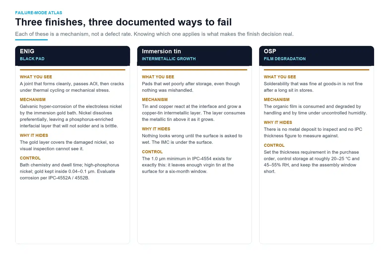
Black pad — also called black nickel — is the reason IPC-4552A and 4552B added corrosion evaluation. The mechanism is galvanic hyper-corrosion of the electroless nickel by the immersion gold bath. Preferential dissolution of nickel leaves a phosphorus-enriched interfacial layer that is neither solderable nor mechanically sound.
What makes it dangerous is the sequence. The gold layer covers the damaged nickel, so the board passes visual inspection. Solder joints form normally during reflow. The joint then cracks or delaminates later — under mechanical stress or thermal cycling, frequently in the field rather than on the line. By the time the symptom appears, the finish that caused it is buried under a solder joint.
Several process variables drive the risk, and they are the ones worth agreeing with your supplier before the order runs:
- Bath condition. Low gold concentration, higher acidity and extended dwell time in an aggressive bath all increase attack on the nickel.
- Nickel phosphorus content. High-phosphorus deposits (roughly 9.5–13 wt%) show less susceptibility to corrosive attack from the immersion gold reaction than mid-phosphorus deposits (roughly 7–9 wt%).
- Deposited gold thickness. Thicker gold means longer exposure, which means more opportunity for corrosion.
How the corrosion is graded
IPC-4552A introduced a corrosion chart: the ENIG surface is examined under an optical microscope at 1000x magnification, and the spikes are graded in frequency and depth across three levels, with Level 3 defined as more than ten spike defects deeper than two microns. IPC-4552B, issued in 2021, kept those levels but added a way to quantify how often defects occur, through a “Product Rating” from 0 to 3 based on examination of seven defined locations in a plated through-hole or five locations on a surface pad.
This matters practically because a board can pass every thickness requirement and still have compromised nickel integrity. Thickness measurement alone does not confirm freedom from black pad. If your application is reliability-critical, the corrosion criteria belong in your purchase specification alongside the thickness numbers.
Where ENIG is the right answer. Fine-pitch components and area-array packages that need flat pads, boards with a long or unpredictable storage window, mixed assembly that includes test probing, and applications where non-destructive thickness verification is a requirement. It is the most broadly capable finish in the group, which is exactly why its failure mode deserves attention instead of assumption.
04 ENEPIG: When the Pad Has to Be Wire Bonded
One extra layer, one extra process step, and access to a different assembly method.
ENEPIG inserts an electroless palladium layer between the nickel and the gold. The specification is IPC-4556, first issued in 2013, with thicknesses set at nickel 3–6 µm, palladium 0.05–0.30 µm, and gold a minimum of 0.03 µm with no upper limit.
That original version had the same gap ENIG had before 2017, and it was closed the same way. A 2015 amendment added an upper limit on gold, capping it at 0.07 µm. The amendment also named the escape route: if a design genuinely requires thicker gold, the specification points to alternative deposition methods — electroless gold or reduction-assisted immersion gold — rather than pushing the immersion gold thickness past the cap.
What the palladium layer buys you
The palladium layer changes what the finished pad is compatible with. ENEPIG is the finish to specify when the same board has to be soldered and gold wire bonded, because the palladium provides a bonding surface that a plain nickel-immersion-gold stack does not offer as reliably. IPC-4556 is unusually thorough on this point: its appendices document round-robin studies covering wetting balance testing, solder spread testing, shear testing, and a dedicated gold wire bonding study — the kind of evidence base you want behind a decision that is expensive to reverse.
All thickness measurements in the specification are taken on a nominal pad of 1.5 mm × 1.5 mm or equivalent area, which matters more than it sounds. Measuring a thin palladium and gold stack by X-ray fluorescence is harder than measuring ENIG, and IPC-4556 devotes an appendix specifically to instrument setup and detector limitations for thin gold and palladium layers.
| Layer | ENIG (IPC-4552A) | ENEPIG (IPC-4556, as amended 2015) |
|---|---|---|
| Electroless nickel | 3–6 µm | 3–6 µm |
| Electroless palladium | — | 0.05–0.30 µm |
| Immersion gold | 0.04–0.1 µm, upper limit strict | 0.03–0.07 µm |
| Solderable | Yes | Yes |
| Gold wire bondable | Not the intended use | Yes — the reason the finish exists |
| Process steps after nickel | One immersion gold step | Palladium step plus immersion gold step |
The trade is straightforward. ENEPIG adds a deposition step and a third layer to control and measure, in exchange for a surface that supports gold wire bonding on top of normal soldering. If your board is never wire bonded, the palladium layer is cost and complexity with no functional return — and the thinner gold cap gives you less corrosion margin than a well-run ENIG line.
05 HASL and Lead-Free HASL: The Workhorse You Should Stop Specifying for Fine Pitch
The cheapest finish on the list, and the one whose thickness nobody controls to a number.
Hot air solder leveling is the oldest finish still in volume production, and its process explains almost everything about its behaviour. The panel is dipped in molten solder, then passed through a hot air knife that blows the excess off the pads. Historically the bath was a eutectic tin-lead alloy at roughly 63% tin and 37% lead; lead-free versions replace it for boards sold into markets where lead is restricted.
The consequence is the important part: the deposit is formed by removing solder, not by depositing a target thickness. What remains on each pad depends on the volume of solder left after the air knife — pad geometry, panel orientation and airflow all move the number. There is no IPC deposit specification for HASL for the same reason it would be difficult to write one.
Why that rules it out for fine pitch
A leveled solder deposit is rounded, not flat. On a generous pitch the dome is harmless. As pitch shrinks, the same dome becomes a liability in three ways:
- Uneven standoff. A domed pad does not present a consistent plane to a paste deposit or a component lead.
- Paste release and stencil contact. Planarity problems show up at printing and placement before they show up at inspection.
- Coplanarity requirements. Finer pitch and area-array packages demand a pad plane that a leveled deposit cannot guarantee pad to pad.
None of that makes HASL a bad finish. It makes it a finish for a specific job. On boards with comfortable pitch, relaxed coplanarity requirements and cost pressure, HASL is competitive on both price and solderability, and its surface stays solderable through handling that would degrade a thinner finish.
The common mistake is inheritance, not selection. HASL ends up on fine-pitch boards because it was the finish on the previous revision, or because it is the cheapest line on a quote. If your board carries area-array packages or sub-0.5 mm pitch, the finish question is already answered, and the answer is not HASL.
06 OSP: The Flattest Pads and the Only Finish With No Specification
A sub-micron organic film that conforms to the copper it protects.
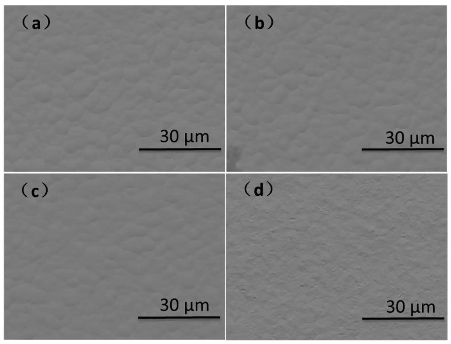
OSP — organic solderability preservative — is not a metal at all. It is a thin organic film that bonds to clean copper and shields it from oxidation. Because the film is sub-micron, commonly applied in the region of 0.2–0.5 µm, and conforms directly to the copper topology rather than building up on it, OSP delivers excellent pad coplanarity — better than any metal finish in this article.
It is also, as covered above, the only common finish with no IPC thickness specification. Work on IPC-4555 ran from 2008 for more than a year and ended without consensus, because the commercially used organic chemistries differ enough in mechanism and recommended thickness that a single set of numbers could not be agreed. The practical consequence is a due-diligence point rather than a defect: if you specify OSP, there is no industry document your supplier can be measured against. The thickness you require has to be stated on the purchase order and controlled by the supplier’s own process monitoring.
Where OSP fits
OSP performs best when the fabrication-to-assembly window is short and known. Its shelf life is the constraint to design around: commonly specified at 6 to 12 months under controlled storage at roughly 20–25 °C and 45–55% relative humidity, and sensitive to how the boards are packaged and handled in between.
It suits high-volume assembly where boards are built and consumed on a schedule, and it avoids the metal-finish concerns that come with silver or gold in some product categories. It is a poor fit for boards that will sit in inventory across a long supply chain, or where the finish has to survive repeated handling and probing before assembly.
07 Immersion Silver and Immersion Tin: The Practical Middle Ground
Both are deposited on copper by the same mechanism, and both specifications carry the scars of getting the numbers wrong.
Immersion silver
Immersion silver deposits silver directly onto copper through a chemical displacement reaction. The specification, IPC-4553, has a history worth knowing because it shows how the industry learned to constrain a finish.
The 2005 original defined two finishes. “Thin” silver had a minimum of 0.05 µm at two sigma with a typical range around 0.07–0.12 µm. “Thick” silver had a minimum of 0.12 µm at four sigma with a typical range around 0.2–0.3 µm. Two specifications for one finish name proved confusing and hard to apply, and the industry converged on one type. IPC-4553A, issued in 2009, replaced both with a single window that for the first time included an upper limit:
- 0.12 µm minimum to 0.4 µm maximum, at plus or minus four sigma from the process mean
- Measured on a pad of approximately 2.25 mm² — for example 1.5 mm × 1.5 mm
- Typical values running between 0.2 and 0.3 µm
The upper limit is the informative part. Capping the deposit stops a supplier from depositing more silver in the belief that more is better, and it keeps the finish inside the window where soldering behaviour is predictable. Where OSP has no specification at all, immersion silver has one with both ends controlled.
Where immersion silver earns its place: fine-pitch boards that need flat pads and good solderability at a cost below the gold-bearing finishes, and applications where silver is acceptable in the finished product. Its shelf life is specified as 12 months when boards are handled and stored according to the specification.
Immersion tin
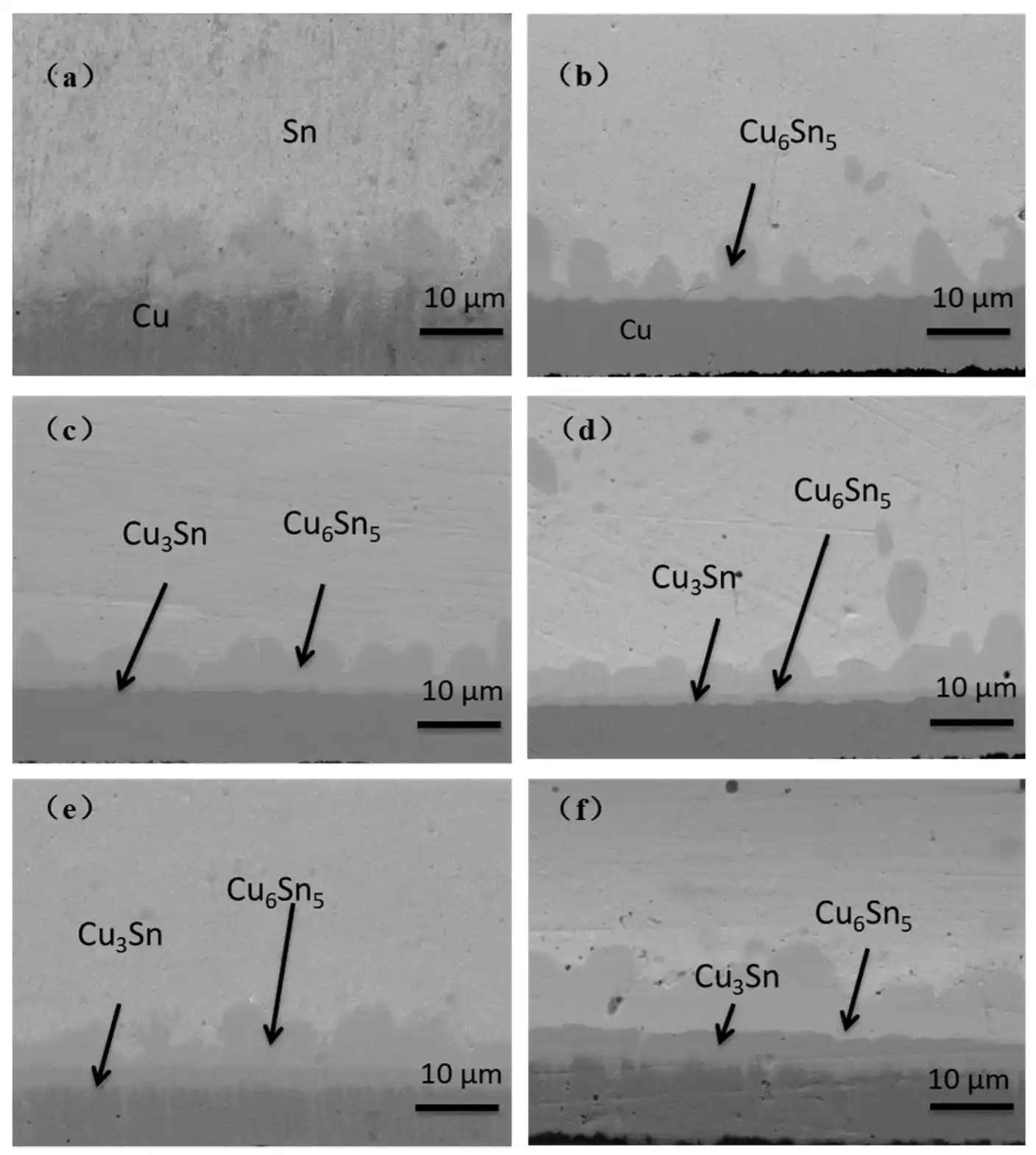
Immersion tin is also deposited by chemical displacement onto copper, and its specification contains the least intuitive number in this article. IPC-4554 requires a minimum of 1.0 µm — 40 microinches at four sigma below the mean, with typical values of 1.15–1.3 µm.
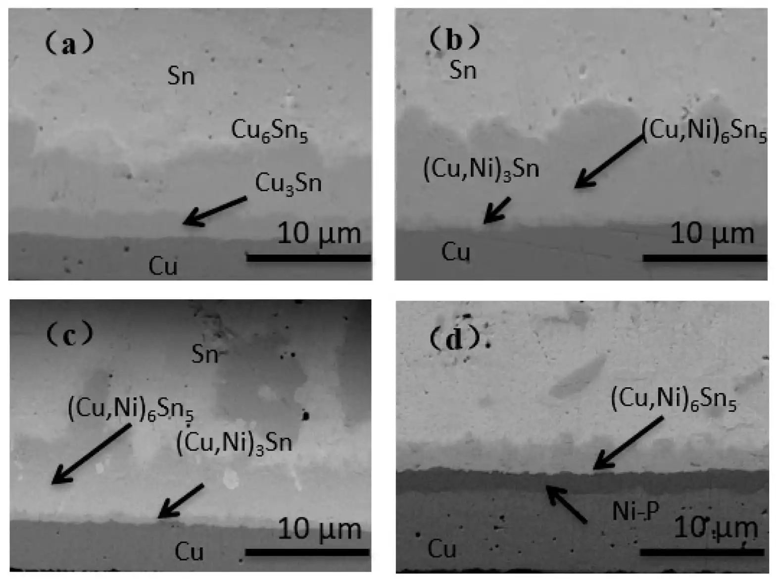
Why so thick, when immersion silver is capped at 0.4 µm? Because tin and copper react. A copper-tin intermetallic layer grows at the interface over time, and it grows at the expense of the metallic tin above it. The committee chose a deposit thick enough that, after storage, enough virgin tin remains at the surface to solder to rather than an intermetallic layer that will not wet. The 1.0 µm minimum is the number that keeps the interface free of copper-tin intermetallic for a six-month shelf life.
A pattern across all four specifications. ENIG got an upper gold limit in 2017. Immersion silver got an upper limit in 2009. ENEPIG got an upper gold limit in 2015. Immersion tin was set by a minimum thick enough to survive storage. In every case the specification moved toward constraining the deposit from both directions, because the industry repeatedly found that more of the surface metal was not better.
08 Hard Gold: A Different Animal
If the surface is going to be inserted, ENIG is the wrong answer.
Hard gold is electroplated nickel and gold, governed by ASTM B488 rather than the IPC final-finish family, typically deposited 0.5–3 µm thick. That is roughly five to thirty times the gold thickness of ENIG, and it is deposited by electroplating — current-driven — rather than by chemical displacement.
The distinction is mechanical, not cosmetic. ENIG gold is thin and soft because it is designed for a single reflow, not for wear. Every insertion cycle of a mated connector erodes gold progressively toward the nickel beneath, and once nickel is exposed the contact resistance rises and the connection degrades. Specifying ENIG for gold fingers or an edge connector is a finish misapplication — and one that no fabrication-stage fix can rescue, because the defect appears only after the board is in service.
| Property | ENIG (immersion gold) | Hard gold (electroplated) |
|---|---|---|
| Deposition method | Chemical displacement | Electroplating |
| Typical thickness | 0.04–0.1 µm | 0.5–3 µm |
| Hardness | Soft | Wear resistant |
| Solderability | Optimized for reflow | Not intended for soldering |
| Intended applications | SMT pads, area-array packages | Gold fingers, edge connectors, mating contacts |
These two are frequently confused in specifications, and the mistake is expensive. Both are described as “gold” on a fabrication drawing, and a drawing that says “gold” without naming the process can be read either way. Name the specification, not the metal: cite IPC-4552 for ENIG pads and ASTM B488 for hard gold contacts.
09 Shelf Life: The Constraint That Outlives the Order
Two boards in the same warehouse age at completely different rates.
Shelf life belongs in the finish decision because the board does not go straight from the fabricator to the reflow oven. It goes to goods-in, to stores, possibly to a contract assembler, possibly to another country. Each finish degrades on its own clock, and the specification states the clock explicitly.
| Finish | Stated shelf life | What sets the limit |
|---|---|---|
| ENIG | 6 months per IPC-4552 against J-STD-003 Category 3 solderability durability; 12 months is the commonly used operational benchmark | Nickel oxidation wherever the gold coverage is thin or discontinuous |
| Immersion silver | 12 months per IPC-4553A when handled and stored to specification | Surface contamination and sulfide attack rather than consumption |
| Immersion tin | Six months minimum, which the 1.0 µm deposit is sized to protect | Growth of the copper-tin intermetallic consuming the metallic tin |
| OSP | Commonly 6–12 months at roughly 20–25 °C and 45–55% relative humidity | Film degradation and handling damage; no IPC figure exists to hold anyone to |
| HASL | Generally the longest of the group | Bulk solder is not consumed the way a thin film is |
The operational point is that a shelf-life number is only meaningful with the storage and packaging conditions attached to it. A 12-month figure assumes controlled temperature and humidity. If your boards will sit in an unconditioned space on the far side of a long supply chain, the specification number is not the number that applies to you.
10 A Decision Framework You Can Defend
Five checks, in the order that eliminates options fastest.
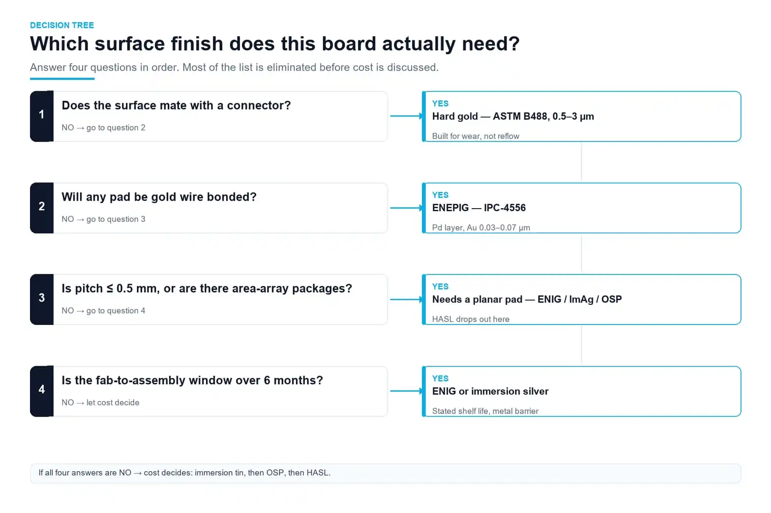
Fine pitch and area-array packages need a planar pad, which removes HASL immediately. Press-fit connectors need a hard, wear-resistant surface, which removes everything except hard gold. The assembly method makes the first cut for you.
Wire bonding pushes toward ENEPIG. Repeated mating contact pushes toward hard gold. A pad that is only ever soldered once does not need either, and paying for them buys nothing.
Not “a few months” — an actual interval from the fabrication date to the assembly date, plus the conditions in between. This is where OSP is usually eliminated, and it is the check most often skipped.
A specification you cannot measure is an aspiration. ENIG and ENEPIG thicknesses are verifiable non-destructively by X-ray fluorescence; OSP has no industry thickness specification to measure against at all. Decide which acceptance numbers you can actually check on the shop floor before you write them down.
Name the IPC specification, not the metal: IPC-4552 for ENIG, IPC-4556 for ENEPIG, IPC-4553A for immersion silver, IPC-4554 for immersion tin, ASTM B488 for hard gold. Where the likelihood of the defect is real, as nickel corrosion is on ENIG, add the corrosion acceptance criteria from IPC-4552B alongside the thickness window.
11 How the Acceptance Criteria Get Checked
The finish is only as good as the measurement behind it.
For ENIG and ENEPIG, the industry-standard non-destructive method is X-ray fluorescence, with the energy-dispersive method for electroless nickel thickness and phosphorus content defined in IPC-TM-650 2.3.44 and measured on a defined 1.5 mm × 1.5 mm feature or equivalent area.
Two practical points decide whether an XRF reading means anything:
- The instrument has to be set up for a multilayer stack. ENIG is gold over nickel-phosphorus over copper. The measurement must resolve signals from all three, which requires multilayer software, correct collimator selection, and calibration standards matched to the actual coating stack. A generic single-layer gold standard cannot do it.
- One reading does not characterise a board. Edge pads and centre pads can differ. Sample across the panel, and treat the specification’s statistical basis — a minimum defined at four sigma below the mean — as what it is: a statement about process capability, not about a single pad.
The finish choice ends with a question for your supplier. Not “do you offer ENIG?” — every fabricator does. Ask where their process centres inside the specification window, how often they sample, and whether they evaluate nickel corrosion. A process running at the middle of the nickel range carries more margin than one sitting on the floor, and both will report “in specification” on a certificate.
Q&A Frequently Asked Questions
1Is ENIG better than ENEPIG?
They are for different requirements rather than better or worse. ENIG covers soldering, fine pitch, flat pads and long shelf life. ENEPIG adds gold wire bonding capability at the cost of an extra deposition step and a thinner gold cap. If your board is never wire bonded, ENEPIG buys nothing you can use.
2Why can ENIG gold not simply be made thicker for more protection?
Because the deposition chemistry is the thing that damages the nickel. Longer exposure deposits more gold and corrodes more nickel at the same time, which is why IPC-4552A set a strict upper limit at 0.1 µm. If thicker gold is genuinely required, the specification directs you to electroless gold or reduction-assisted immersion gold instead of extending the immersion step.
3How do I know whether my board has black pad?
You cannot tell from the surface, because the gold covers the corroded nickel. Detection comes from evaluating the nickel corrosion directly — which is what the corrosion chart in IPC-4552A and the Product Rating in IPC-4552B are for — or from solderability and shear testing. Visual inspection of a plated board will not show it.
4Which finish should we use if the board will be stored for an unknown period?
That requirement argues for a finish with a metal barrier and a stated shelf life — ENIG or immersion silver — and against OSP, whose usable window depends on controlled storage and a known assembly date. Whichever you choose, fix the storage conditions in writing, because shelf-life figures are quoted against controlled temperature and humidity.
Choosing a finish? Send us the drawing and the assembly plan.
We review surface finish against pitch, assembly method, storage window and test plan before the order is released — and we tell you where we will centre the process inside the specification window.
Upload Gerber / BOM See the Equipment ListRelated reading: Design Rules vs Fab Capability · AOI, X-ray, Flying Probe and ICT · PCB Lead Time, Decoded · How to Read a PCB Manufacturer’s Equipment List
0users like this.
