


- Contact Us
-
TEL: + 86-13428967267
FAX: + 86-4008892163-239121
+ 86-2028819702-239121
Email: sales@o-leading.com Contact Now
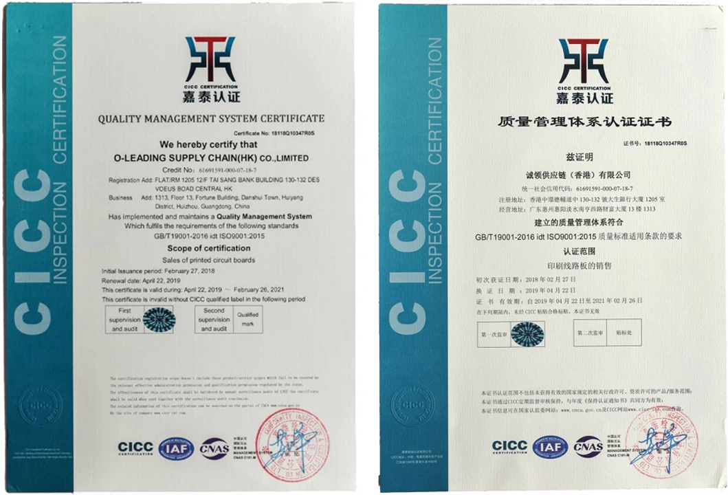
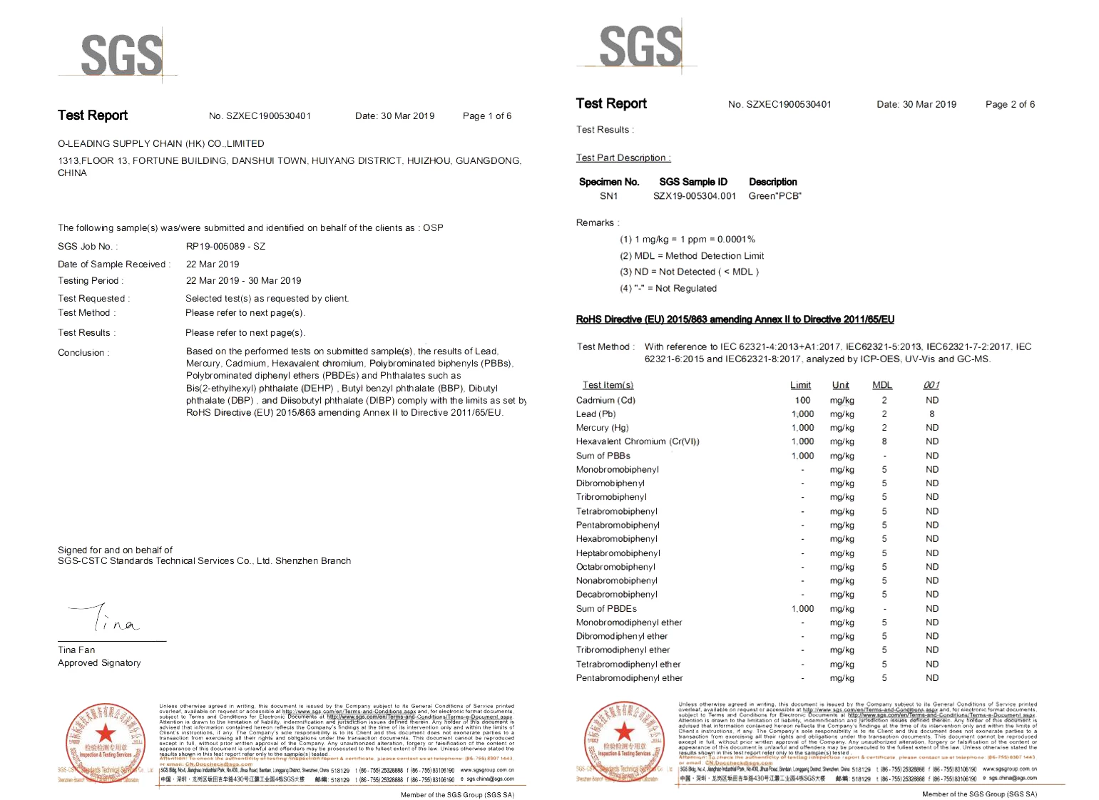
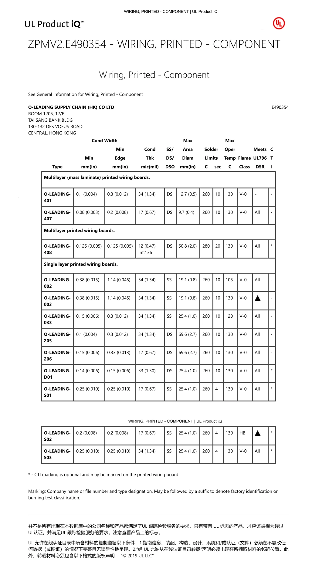
- Certifications
-


- Subscribe
-
Get email updates on new products
- New Products


- Electronic album

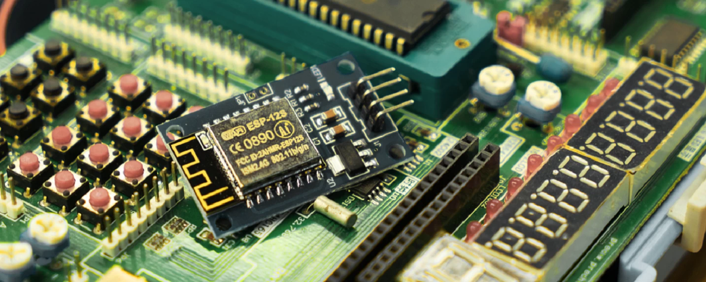
High quality pcb wholesales, Printed circuit board supplier, Pcb design in china
- Layers: 2
- Material: FR4
- Finished Thickness: 1.57mm +/- 10%
- Outer Layer Copper Thickness: 1oz
- Finish: ENIG (Au:2-5u")
- Soldermask (Color): Both Sides, LPI (Black)
- Silkscreen (Color): Both Sides, White
| Welcome to O-leading |
O-Leading strives to be your one stop solution partner in EMS supply chain, including PCB design , PCB fabrication and PCB assembly (PCBA).We provide some of the most advanced PCB technology, including HDI PCBs,multilayer PCBs, Rigid-Flexible PCBs.We can support from quick turn prototype to medium & mass Production.
In general, our global customers are very impressed with our services:rapid response, competitive price and quality commitment.Providing more valuable technical service and overall solution is the way O-leading forward. Printed circuit board supplier
Looking to the future, O-leading will concentrate on the innovation and development of electronics manufacturing technology as always, and make persistent efforts on PCB & PCBA one-stop service to provide first-class services and create more value for our customers.
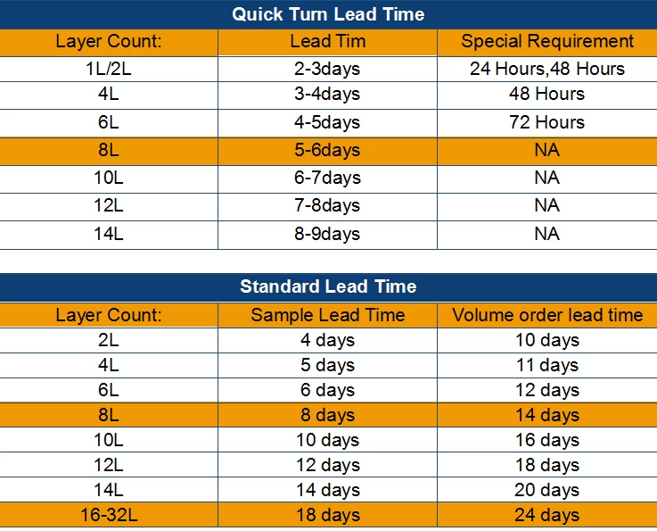
We are professional PCB manufacturer with more than ten years experiences . Products range-single, double side ,multi-layer PCB ,flexible PCB and MCPCB.We can provide fast prototype service – S/S in 24hrs , 4-8layers in 48-96 working hrs production time.
COPPER PLATE HOLES MINIMUM .025 AVG, .020 MIN.. HOLES MAY NOT BE PLUGGED
Pack with colorless transparent bubble film ,25 PCS/ bag, put desiccant in flank, put humidity indicator card on top side
| Product Description |
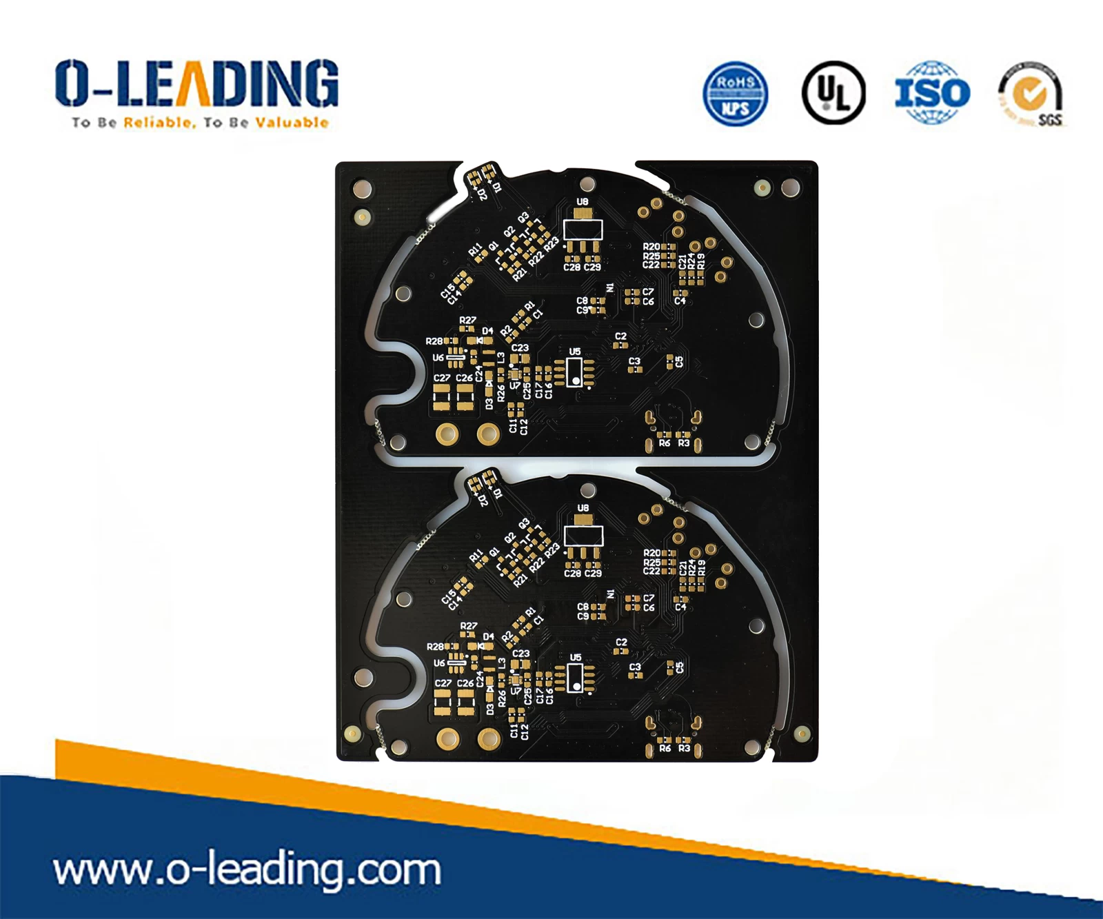
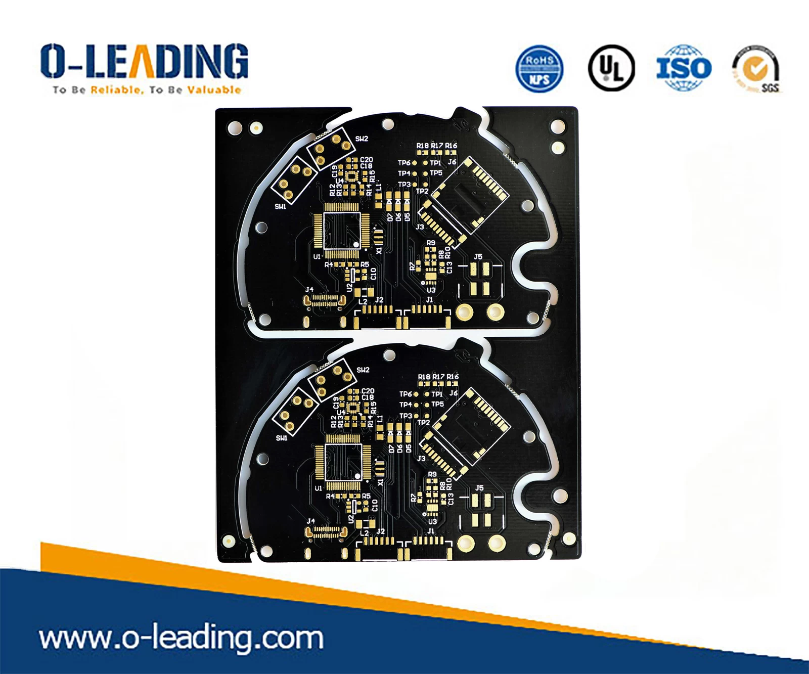
Material: FR4
Finished Thickness: 1.57mm +/- 10%
Outer Layer Copper Thickness: 1oz
Finish: ENIG (Au:2-5u")
Soldermask (Color): Both Sides, LPI (Black)
Silkscreen (Color): Both Sides, White
Electrical test
FINISH: THIS BOARD SHALL BE IMMERSION GOLD PLATED ACCORDING TO IPC-6012.
THICKNESS SHALL BE .050uM OVER 3-6uM NICKEL.
COPPER PLATE HOLES MINIMUM .025 AVG, .020 MIN.. HOLES MAY NOT BE PLUGGED, EXCEPT VIAS .500 FINISH OR SMALLER.
Layer Key:
==========
*.GM4: Board Outline
*.TXT: NC Drill File
*.GTP: Top Paste
*.GTO: Top Silkscreen
*.GTS: Top Soldermask
*.GTL: Top Copper Layer
*.GBL: Bottom Copper Layer
*.GBS: Bottom Soldermask
*.GBO: Bottom Silkscreen
*.GBP: Bottom Paste


| Our Team |
| Certifications |
| Packaging & Delivery |

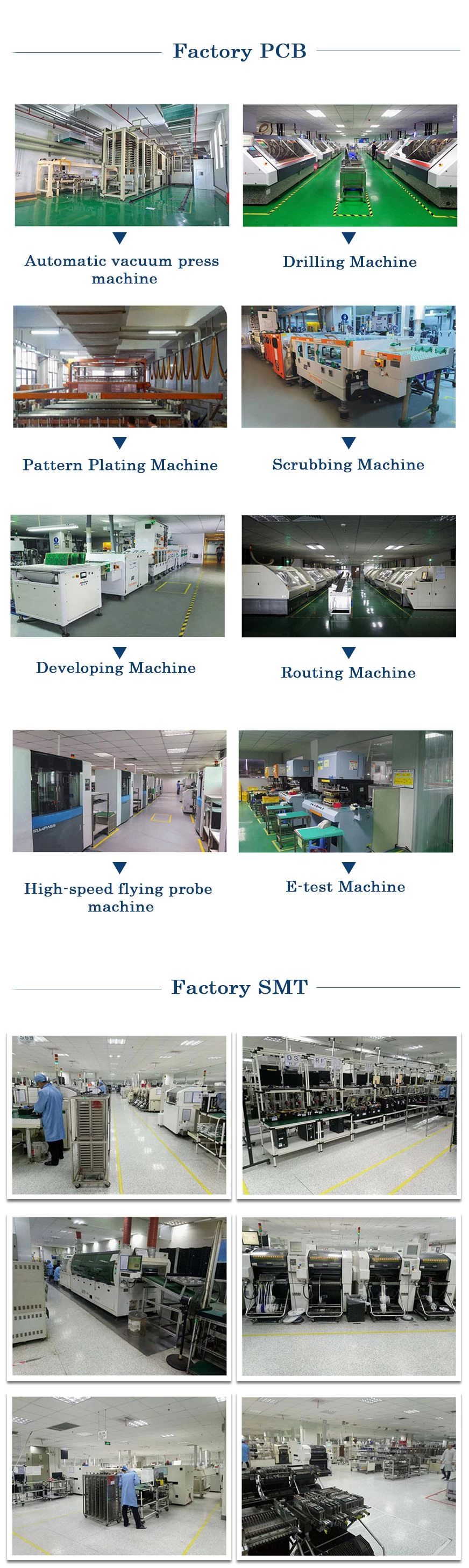
| Process Capability |
SMT Production Capabilities
PCB Material: FR-4,CEM-1,CEM-3,Aluminum-based board
Max PCB size: 510x460mm
Min PCB size:50x50mm
PCB Thickness:0.5mm-4.5mm
Board thickness:0.5-4mm
Min Components size: 0201
Standard chip size component: 0603 and larger
Component max height:15mm
Min lead pitch: 0.3mm
Min BGA ball pitch:0.4mm
Placement precision: +/-0.03mm
Tag:
Double-side
- Other Products


