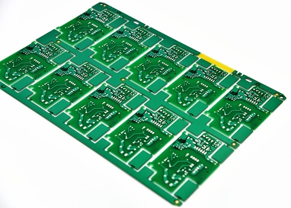
PCB prototype first step in the fabrication process is usually to find the material of the pcb
o-leading.com
o-leading.com
2017-04-27 12:09:53
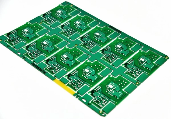
Following your material continues to be selected, the 1st process is to apply a coating of copper for the entire board. The circuit layout will then be printed about the board with a photosensitive process. Then, a photograph engraving process will probably be used to ensure all of the copper that isn't part of the circuit layout will be etched out or taken out of the board. The resulting copper produces the traces or tracks with the PCB circuit. To get in touch the circuit traces, two processes are used. A mechanical milling process uses CNC machines to take out the unwanted copper from the board. Then, an etch-resistant, silk-screen, printing process is applied to hide the regions where traces must exist.