


Anti interference measures for printed circuit boards
o-leading.com
o-leading.com
2017-07-28 19:10:14
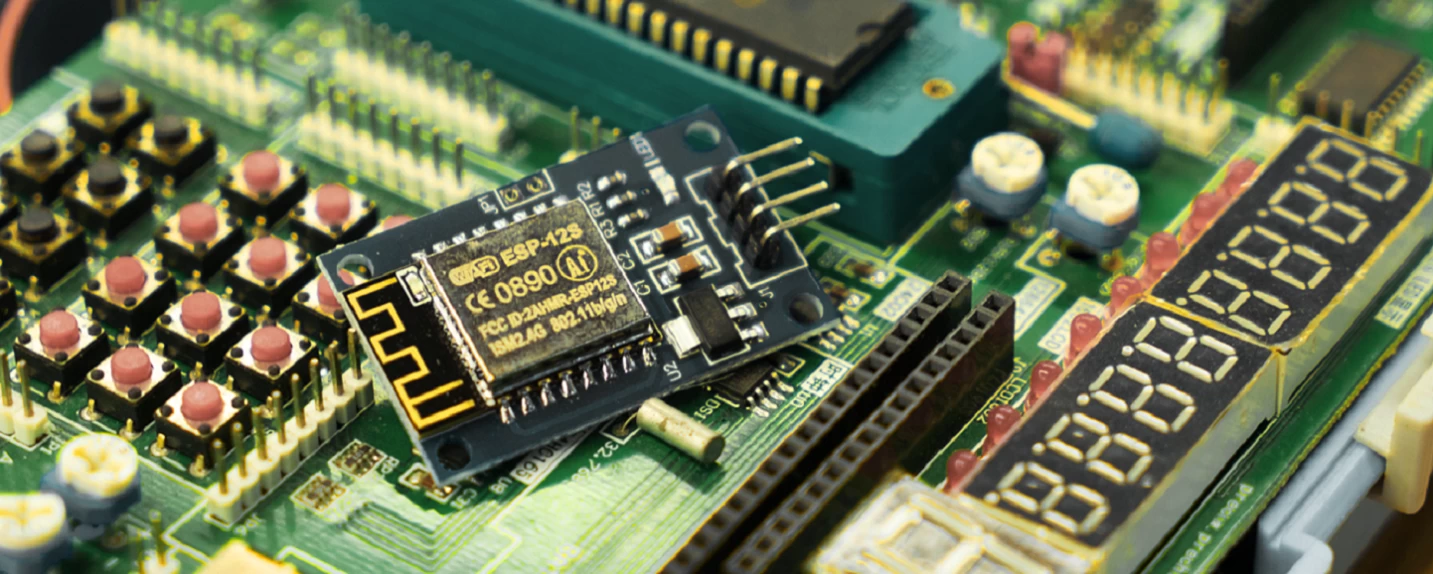
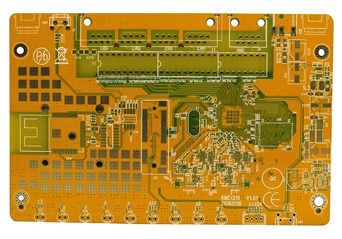
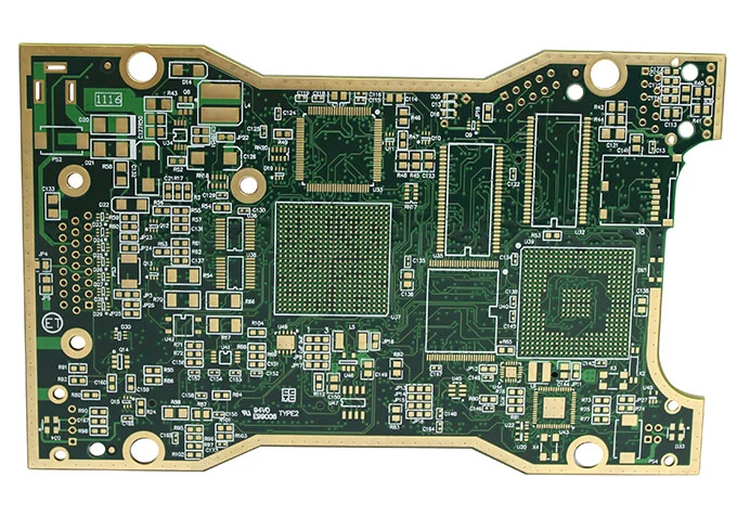
The anti-interference design of printed circuit board is closely related to the specific circuit. Here, some common measures of PCB (oem pcb board manufacturer china) anti-interference design are explained.
1. power cord design
According to the printed circuit board current size, as far as possible leased power line width, reduce loop resistance. Meanwhile, the direction of the power line and the ground wire is consistent with the data transmission direction, so that the anti noise capability can be enhanced.
2. ground design
Ground design is the principle of:
(1) separate from analog to digital. If there are logic circuits and linear circuits on the circuit board (china pcb manufacturer), they should be separated as far as possible. The low frequency circuit should try to adopt single point parallel connection, and when the actual wiring is difficult, it can be connected in series and connected again.
(2) grounding wire should be as bold as possible. If the ground with a sewing line, then the ground potential change with the current change, the anti noise performance decreased.
(3) the grounding wire forms the closed loop. A printed circuit board (HDI pcb Printed circuit board) consisting of a digital circuit, whose grounding circuit is made up of a group loop, can largely improve the noise immunity.