


Super useful! Three tips on the reduction of pcb design risk
o-leading.com
o-leading.com
2017-06-01 15:14:45
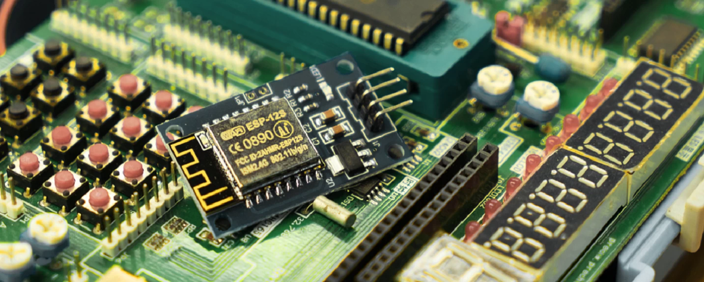
Pcb design in china, if we can predict the possible risk in advance, we can advance to prevent risks, improve the success rate of PCB design. The key to improving the success rate of a board lies in the design of signal integrity. The current electronic system design has a lot of product solutions, chip manufacturers have done, including the use of what chip, how to build a peripheral circuit and so on. Hardware engineers often do not need to consider the circuit principle of the problem, only need to make their own PCB.
But many china Pcb design company have encountered problems in the PCB design process, either PCB design out of instability, or not work. For large enterprises, many chip manufacturers will provide technical support for PCB design guidance. But some small and medium enterprises are difficult to get this support. Therefore, we must find a way to complete their own, so there have been many problems, may need to play several versions, debugging for a long time. In fact, if you understand the system design methods, which can be avoided. Then we come to introduce the three tips on reducing the risk of PCB design.
First, the system planning stage to consider the signal integrity of the problem, the whole system to build such a signal from a PCB to another PCB can not be properly received? It is necessary to assess the early, and the assessment of this problem is not difficult, understand the signal integrity of knowledge, will be a little simple software operation can do.
Second, in the PCB design process, the use of simulation software to assess the specific alignment, observe the signal quality can meet the requirements, the simulation process itself is very simple, the key is to understand the principle of signal integrity knowledge, and used to guide.
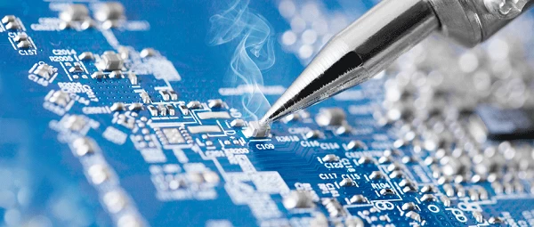
Third, do the Circuit board manufacturing, we must carry out risk control. There are many problems, the current simulation software has no way to solve, must be designed by the designer. The key to this step is to understand where there is risk, how to do it to avoid the risk, need or signal integrity knowledge.
If you can grasp the three points in the PCB design process, then you can reduce the PCB design risk, the probability of boarding board will be lower, debugging is relatively easy.
First, the system planning stage to consider the signal integrity of the problem, the whole system to build such a signal from a PCB to another PCB can not be properly received? It is necessary to assess the early, and the assessment of this problem is not difficult, understand the signal integrity of knowledge, will be a little simple software operation can do.
Second, in the PCB design process, the use of simulation software to assess the specific alignment, observe the signal quality can meet the requirements, the simulation process itself is very simple, the key is to understand the principle of signal integrity knowledge, and used to guide.
Third, do the Circuit board manufacturing, we must carry out risk control. There are many problems, the current simulation software has no way to solve, must be designed by the designer. The key to this step is to understand where there is risk, how to do it to avoid the risk, need or signal integrity knowledge.
If you can grasp the three points in the PCB design process, then you can reduce the PCB design risk, the probability of boarding board will be lower, debugging is relatively easy.