


The use and interpretation of PCB industry terminology
o-lead
o-leading.com
2018-05-16 11:58:44
The world is divided into parts that work with the metric system and define the part of the measurement together with the empire system. "μm" is 25.4 times smaller than "Mil". The size of electronic products has been shrinking. To ensure the highest quality, we decided many years ago to specialize in metric system work in the front-end department. Therefore, the basis for all measurements given in this document and our website is the metric system. All empire values are only for clarification and general understanding.
The global PCB industry has no universal consensus on terms, so if we feel that any terminology we use may not be clear, we try to explain it when we first see it.
Input data format
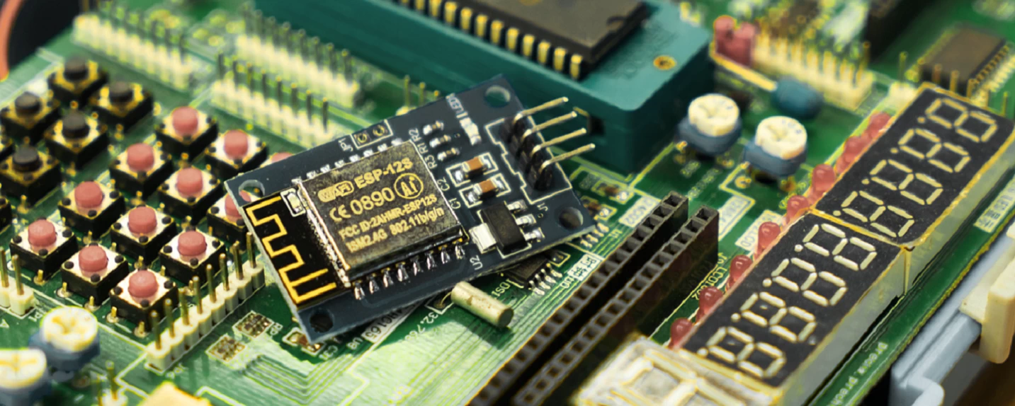
The acceptable data format for PCB layout data is:
Process:
Gerber version 2 (or Gerber X2) or Gerber version 1 (or Geber X1). All Gerber specifications come from the Ucamco NV owner's format.
DPF (Dynamic Process Format - developed by Ucamco NV)
Eagle.BRD file (CAD data from CADsoft now Premier Farnell)
The process means all copper layers, solder mask and legend layers, circuit board outlines or mechanical layers, SMD solder paste layers, carbon layers, peel layers, and so on.
Excellon (1 or 2) + Appropriate list of tools (ideally embedded)
Sieb & Meyer + Appropriate Tool List (ideally embedded)
Gerber format (only true borehole data, not borehole maps)
DPF (only drill data, not drilling maps).
The use and interpretation of PCB industry terminology
important:
Please only provide ASCII-coded files. These files are readable so that our engineers can visually inspect them as needed during data preparation. So we do not accept formats such as EIA or EBCDIC. We prefer the Gerber X2.
We do not accept native CAD PCB design data other than EAGLE or KiCAD.
1. Converting CAD data into production data may result in errors and we cannot cross-check. 2. A legal copy of each CAD PCB design package cannot be obtained in the market and the necessary knowledge to use them correctly cannot be obtained. Since designers do not all use the same software version, we also need a full set of update patches.
Gerber is clear and clear. For years, it has been the industry standard format for PCB manufacturing. Each PCB design package can output Gerber data. This process will be fully described in your CAD PCB(Printed circuit board in china)design package manual or help file.