


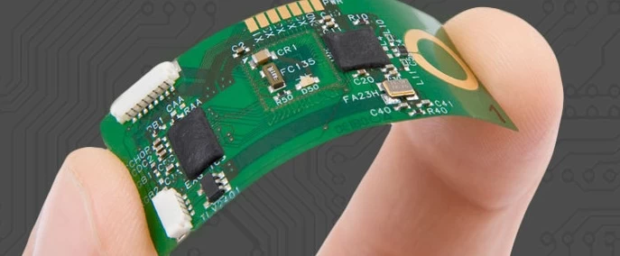
PCB Design Collection: How can an electronic engineer not draw a PCB board?
o-leading
o-leading.com
2018-03-23 21:04:55
For those who are determined to be electricians, the drawing board is hard and martial arts. If you don't practice, you won't be successful. Even if you can record all the characteristics of the MOS tube, it will eventually become ineffective.
The basic PCB design flow is as follows: Preliminary preparation - "PCB structure design -" PCB layout - "wiring -" wiring optimization and silk screen - "Network and DRC inspection and structural inspection -" plate.

1 early preparation
This includes preparing component libraries and schematics. "For a worker to be good at something, he must first sharpen his tools." To make a good board, in addition to designing principles, he must paint well. Before doing PCB design, we must first prepare the schematic SCH's component library and PCB's component library. Component library can use peotel's own library, but in general it is difficult to find a suitable, it is best that they do their own component library based on the standard size of the selected device. In principle, first do the PCB's component library, and then do SCH's component library. The requirements of the PCB's component library are relatively high. It directly affects the installation of the board. The SCH's component library requirements are relatively loose, as long as you pay attention to defining the pin attributes and the corresponding relationship with the PCB components. PS: Note the hidden pins in the standard library. After that is the schematic design, ready to start doing PCB design.
2PCB structural design
In this step, according to the determined circuit board size and various mechanical positioning, the PCB board surface is drawn in the PCB design environment, and the required connectors, buttons/switches, screw holes, assembly holes, etc. are placed according to the positioning requirements. And fully consider and determine the wiring area and non-wiring area (for example, the extent of screw holes around the non-routing area)
3PCB layout
To put it plainly, it means putting devices on the board. At this time, if the preparations mentioned above are all done well, you can create a netlist (Design->Create Netlist) on the schematic, and then import the netlist (Design->Load Nets) on the PCB diagram. I saw all the parts of the device crashing up, and there are flying lines between the pins. Then you can layout the device. The general layout is as follows:
1 According to the reasonable partition of electrical performance, generally divided into: digital circuit area (that is, fear of interference, but also produce interference), analog circuit area (fear of interference), power drive area (interference source);
2 The circuit that completes the same function should be placed as close as possible, and adjust the components to ensure the connection is the most concise; at the same time, adjust the relative position between the functional blocks to make the connections between the functional blocks the most concise;
3 For high-quality components, the installation location and installation strength should be considered; heating elements should be placed separately from temperature-sensitive components, and thermal convection measures should also be considered when necessary;
4 I/O driving device as close as possible to the edge of the printed board, close to the outgoing connector;
5 The clock generator (such as crystal or clock) should be as close as possible to the device that uses this clock;
6 Between each power supply input pin of the integrated circuit and ground, a decoupling capacitor (usually a monolithic capacitor with good high frequency performance) is needed; when the circuit board space is dense, it can also be added around several integrated circuits. A tantalum capacitor.
7 Add a discharge diode (1N4148) to the relay coil;
8 Layout requirements should be balanced, dense and orderly, not top-heavy or heavy - need special attention, when placing the device, we must consider the actual size of the components (area and height), between the components Relative position, in order to ensure the electrical performance of the circuit board and the feasibility and convenience of production and installation at the same time, should ensure that the above principles can be reflected on the premise of appropriate modification of the device placement, so that it is neat and beautiful, such as the same device to be placed Put it neatly and in the same direction, and you can't put it in a "catch-up." This step is related to the overall image of the board and the ease of wiring in the next step, so we must take great efforts to consider. When laying out, you can make preliminary wiring and fully consider where you are not sure.
The basic PCB design flow is as follows: Preliminary preparation - "PCB structure design -" PCB layout - "wiring -" wiring optimization and silk screen - "Network and DRC inspection and structural inspection -" plate.
1 early preparation
This includes preparing component libraries and schematics. "For a worker to be good at something, he must first sharpen his tools." To make a good board, in addition to designing principles, he must paint well. Before doing PCB design, we must first prepare the schematic SCH's component library and PCB's component library. Component library can use peotel's own library, but in general it is difficult to find a suitable, it is best that they do their own component library based on the standard size of the selected device. In principle, first do the PCB's component library, and then do SCH's component library. The requirements of the PCB's component library are relatively high. It directly affects the installation of the board. The SCH's component library requirements are relatively loose, as long as you pay attention to defining the pin attributes and the corresponding relationship with the PCB components. PS: Note the hidden pins in the standard library. After that is the schematic design, ready to start doing PCB design.
2PCB structural design
In this step, according to the determined circuit board size and various mechanical positioning, the PCB board surface is drawn in the PCB design environment, and the required connectors, buttons/switches, screw holes, assembly holes, etc. are placed according to the positioning requirements. And fully consider and determine the wiring area and non-wiring area (for example, the extent of screw holes around the non-routing area)
3PCB layout
To put it plainly, it means putting devices on the board. At this time, if the preparations mentioned above are all done well, you can create a netlist (Design->Create Netlist) on the schematic, and then import the netlist (Design->Load Nets) on the PCB diagram. I saw all the parts of the device crashing up, and there are flying lines between the pins. Then you can layout the device. The general layout is as follows:
1 According to the reasonable partition of electrical performance, generally divided into: digital circuit area (that is, fear of interference, but also produce interference), analog circuit area (fear of interference), power drive area (interference source);
2 The circuit that completes the same function should be placed as close as possible, and adjust the components to ensure the connection is the most concise; at the same time, adjust the relative position between the functional blocks to make the connections between the functional blocks the most concise;
3 For high-quality components, the installation location and installation strength should be considered; heating elements should be placed separately from temperature-sensitive components, and thermal convection measures should also be considered when necessary;
5 The clock generator (such as crystal or clock) should be as close as possible to the device that uses this clock;
6 Between each power supply input pin of the integrated circuit and ground, a decoupling capacitor (usually a monolithic capacitor with good high frequency performance) is needed; when the circuit board space is dense, it can also be added around several integrated circuits. A tantalum capacitor.
7 Add a discharge diode (1N4148) to the relay coil;
8 Layout requirements should be balanced, dense and orderly, not top-heavy or heavy - need special attention, when placing the device, we must consider the actual size of the components (area and height), between the components Relative position, in order to ensure the electrical performance of the circuit board and the feasibility and convenience of production and installation at the same time, should ensure that the above principles can be reflected on the premise of appropriate modification of the device placement, so that it is neat and beautiful, such as the same device to be placed Put it neatly and in the same direction, and you can't put it in a "catch-up." This step is related to the overall image of the board and the ease of wiring in the next step, so we must take great efforts to consider. When laying out, you can make preliminary wiring and fully consider where you are not sure.
For more information about PCB NEWS, please click the link Printed circuit board supplier.
TEL: + 86-13428967267
FAX: + 86-4008892163-239121
+ 86-2028819702-239121
Email: sales@o-leading.com
TEL: + 86-13428967267
FAX: + 86-4008892163-239121
+ 86-2028819702-239121
Email: sales@o-leading.com