


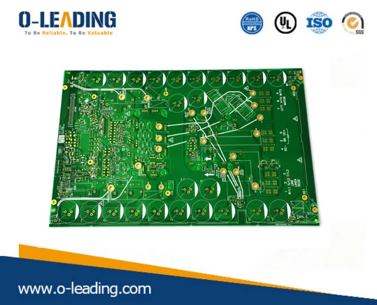
How to place RF circuit and digital circuit on a PCB?
o-leading.com
o-leading.com
2017-11-09 15:51:36
Monolithic RF devices greatly facilitate the field of wireless communications within a certain range of applications, the use of suitable microcontrollers and antennas combined with the transceiver device can form a complete wireless communications link. They can be integrated in a small circuit board for wireless digital audio, digital video data transmission systems, wireless remote control and telemetry systems, wireless data acquisition systems, wireless networks and wireless security systems and many other areas.
Potential conflicts between digital and analog circuits
If analog circuits (radio frequency) and digital circuits (microcontrollers) work individually, they may each work well, but once the two are on the same board, working together on the same power supply, the entire system is likely to be unstable . This is mainly because the digital signal frequently swings between the ground and the positive supply (3V in size), and the cycle is extremely short, often at the ns level. Due to the larger amplitude and the smaller switching times, these digital signals contain a large number of high-frequency components independent of the switching frequency. In the analog part, the signal from the antenna tuning loop to the receiving part of the wireless device is generally less than 1μV. Therefore, the difference between the digital signal and the RF signal will reach 10-6 (120dB). Obviously, if the digital signal and the RF signal can not be well separated, the faint RF signal may be damaged, so the working performance of the wireless device will be worsened, or even completely unable to work.
RF circuits and digital circuits on the same PCB PCB common problems
Inadequate isolation of sensitive lines and noise signal lines is a common problem. As mentioned above, the digital signal has a high swing and contains a large amount of high-frequency harmonics. If the digital signal on the PCB is routed close to sensitive analog signals, high frequency harmonics may couple past. The most sensitive nodes of an RF device are usually the loop-filter circuit of a phase-locked loop (PLL), the external voltage-controlled oscillator (VCO) inductor, the crystal reference signal, and the antenna terminals. These parts of the circuit should be handled with particular care.