


Wow! Five layout requirements of PCB board components
o-leading.com
o-leading.com
2017-06-05 11:15:50
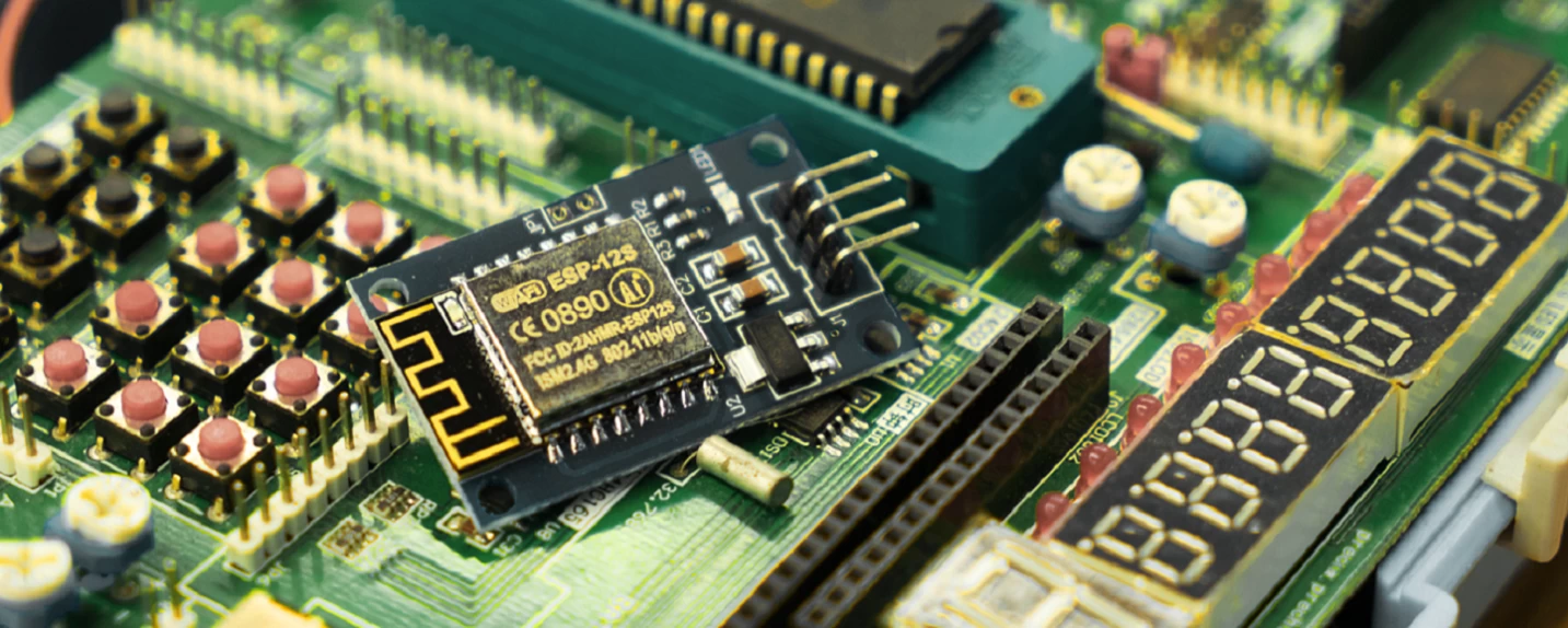
The rational layout of the Custom Circuit Boards china components in the patch processing is the basic premise of designing the high quality PCB diagram. On the requirements of the main components of the installation, stress, heat, signal, beautiful five requirements.
Second, the force, the chip processing circuit board should be able to withstand the installation and work suffered a variety of external forces and vibration. For this circuit board should have a reasonable shape, the board of various holes (screw holes, shaped holes) the location to be reasonable arrangements. The distance between the hole and the edge of the hole is at least greater than the diameter of the hole. Also note that the weakest cross section of the plate caused by the profiled hole should also have sufficient bending strength. The board directly "stretch" out of the device shell connector in particular to be a reasonable fixed, to ensure long-term use of reliability.
Third, the heat, for high-power, serious heat of the device, in addition to guarantee the cooling conditions, but also pay attention to place in the appropriate location. Especially in precision analog systems, pay particular attention to the adverse effects of the temperature field generated by these devices on the fragile preamplifier circuit. General power is very large part of the module should be made alone, and with the signal processing circuit to take a certain degree of thermal isolation measures.
 Fourth, the signal, the signal interference PCB layout design to consider the most important factor. The most basic aspects are: weak signal circuit and strong signal circuit separately or even isolated; AC part and DC part of the separation; high frequency part and low frequency part of the separation; pay attention to the signal line to the direction of the ground; appropriate shielding, filtering And other measures.
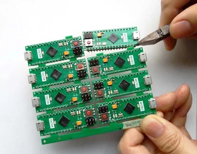
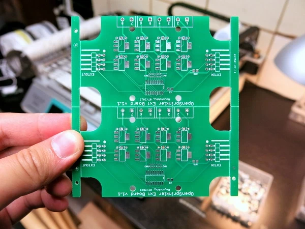
First, the installation, refers to the specific application, in order to install the circuit board into the chassis, shell, slot, no interference occurs, short circuit and other accidents, and make the specified connector in the chassis or shell on the specified location Made a series of basic requirements.
Second, the force, the chip processing circuit board should be able to withstand the installation and work suffered a variety of external forces and vibration. For this circuit board should have a reasonable shape, the board of various holes (screw holes, shaped holes) the location to be reasonable arrangements. The distance between the hole and the edge of the hole is at least greater than the diameter of the hole. Also note that the weakest cross section of the plate caused by the profiled hole should also have sufficient bending strength. The board directly "stretch" out of the device shell connector in particular to be a reasonable fixed, to ensure long-term use of reliability.
Third, the heat, for high-power, serious heat of the device, in addition to guarantee the cooling conditions, but also pay attention to place in the appropriate location. Especially in precision analog systems, pay particular attention to the adverse effects of the temperature field generated by these devices on the fragile preamplifier circuit. General power is very large part of the module should be made alone, and with the signal processing circuit to take a certain degree of thermal isolation measures.
We are Thick copper pcb wholesales china and Quick turn pcb Printed circuit board, if you like our products, contact us.